A BULK-DRIVEN CMOS OTA WITH 68 dB DC GAIN Jonathan Rosenfeld, Mücahit Kozak, and Eby G. Friedman Department of Electrical and Computer Engineering University of Rochester Rochester, New York 14627-0231 manner, the threshold voltage of a MOSFET can be reduced or even removed from the signal path.
ABSTRACT An ultra-low voltage rail-to-rail operational transconductance amplifier (OTA) based on a standard digital 0.18 !m CMOS process is described in this paper. Techniques for designing a 0.8 volt fully differential OTA are discussed including bias and reference current generator circuits. To achieve rail-to-rail operation, complementary input differential pairs are used, where the bulk-driven technique is applied to reduce the threshold limitation of the MOSFET transistors. The OTA gain is increased by using auxiliary gain boosting amplifiers. This additional circuitry enables the OTA to operate at 0.8 volts, achieving an open loop gain of 68 dB while consuming 94 !W. The DC gain of the amplifier is the highest gain achieved to date in bulk-driven amplifiers. *
The concept of a bulk-driven MOS transistor was first proposed by Guzinski et al. in 1987 [1] as active components in an OTA differential input stage. Later, in 1991, the concept was used in the practical realization of a software-programmable CMOS telephone circuit [2]. However, not until 1998 [3] did the method draw significant attention as a viable low-voltage analog design technique. Specifically, in [3], a 1 volt Op Amp was designed in a standard CMOS digital process utilizing the depletion characteristics of bulk-driven transistors. One important drawback of the bulk-driven method, however, is that the body transconductance gmb is approximately five times smaller than the gate transconductance gm. Thus, when the input differential pair of an amplifier is composed of bulk-driven transistors, the resulting DC gain is relatively low. This behavior is the primary reason for the low gain (around 45 dB) in previously reported bulk-driven amplifiers [3], [4].
1. INTRODUCTION The reduction in the minimum dimensions in VLSI technologies along with the trend of using small portable devices necessitates reduced power supply voltages. In order to facilitate submicrometer high density systems on a single integrated circuit (IC), voltage levels must be lowered to ensure reliability. Threshold voltages of future CMOS technologies may not decrease much below what is available today, making it difficult to design analog circuits with lower supply voltages.
In this paper, a 0.8 volt fully differential folded-cascode OTA is presented. Both PMOS and NMOS bulk-driven input differential pairs are used to achieve full rail-to-rail operation. A continuoustime common mode feedback circuit is adopted in order to suppress variations in the output common mode. Four commonsource gain boosting amplifiers are used to increase the gain to the target level of 68 dB (the DC gain was around 48 dB before gain boosting). This gain is the highest gain achieved to date in bulk-driven amplifiers. A bias circuitry which generates the required bias voltages for the amplifier core along with a low sensitive reference current generator circuit are also presented
In analog circuit design, the threshold voltage of a transistor should be lowered in proportion to the reduction in the supply voltage to appropriately bias the device. This characteristic makes standard low voltage analog circuits incompatible with CMOS technology trends. To combat this conflict without requiring the development of expensive CMOS technologies with lower threshold voltages, novel circuit design techniques must be developed that are compatible with future CMOS technologies.
This paper is organized as follows. The design of the amplifier core is presented in Section 2. In Section 3, the bias circuit and reference current generator are described. In Section 4, the circuit layout is presented. In section 5, the performance of the amplifier is summarized and some conclusions are offered in Section 6.
A promising approach in low voltage analog circuits is the socalled “bulk-driven” MOSFET method. In this method, the gateto-source voltage is set to a value sufficient to form an inversion layer, and an input signal is applied to the bulk terminal. In this
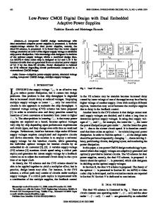
2. THE AMPLIFIER CORE The amplifier core of an OTA is illustrated in Figure 1. This circuit is based on a fully differential topology with two complementary input pairs. The output branch consists of common gate amplifiers with cascode current loads to increase the gain. A common mode feedback circuit is used with four auxiliary common source amplifiers. The operation of the OTA is explained in greater detail below.
*
This research was supported in part by the Semiconductor Research Corporation under Contract No. 2003-TJ-1068, the DARPA/ITO under AFRL Contract F29601-00-K-0182, the National Science Foundation under contract No. CCR-0304574, the Fullbright Program under Grant No. 87481764, grants from the New York State Office of Science, Technology & Academic Research to the Center for Advanced Technology – Electronic Imaging Systems and to the Microelectronics Design Center, and by grants from Xerox Corporation, IBM Corporation, Intel Corporation, Lucent Technologies Corporation, and Eastman Kodak Company.
0-7803-8715-5/04/$20.00 ©2004 IEEE.
2.1 Rail-to-Rail Operation Rail-to-rail operation is achieved using a pair of PMOS (M5 and M6) and NMOS (M33 and M34) transistors at the input stage. This
5
VDD !
!
!
!
!
M13
Vref _ cm M 25
M 24
!
M 26
M 27
!
!
!
M 14
!
N ! type CS amp.
! !
!
! !
M 17
! !
!
!
Vb1
M 19
!
Vb 3
M 23 ! !
VDD
!
!
!
M 28
Vb 2
VDD
!
P ! type CMFB
NMOS input pair !
M 18
M 20 Vb 4
M9
!
M 33
!
!
M10
Vin!
!
M 34
Vb 7
Vin!
!
M 38 !
VDD
!
V
! out
!
M5 V
! in
M6 V
! in
!
M 15
! !
M7
M8
! !
!
!
! ! !
!
PMOS input pair
V
Vb 5
N ! type CMFB M 21
M 37
M 32
! !
Vb 6
M 16
!
" out
M 22
!
! !
! !
M 29
Vb1 !
M3
P ! type CS amp.
M4
!
M 30
!
M 31
!
M 36
!
! !
!
M 35
Vref _ cm !
!
!
!
Figure 1. The amplifier core of an OTA
strategy supports rail-to-rail (0 volt to 0.8 volt) operation of the amplifier, thus the input common mode range (ICMR) is extended to the largest possible range. This increased range is achieved since when the input common mode voltage is low, the P-type pair is on and the N-type pair is off (when the input common mode is high, the P-type pair is off and the N-type pair is on). In the middle range, however, both pairs are on, providing a higher overall gain.
more overdrive voltage to maintain the transistors in the saturation region, while simultaneously increasing the voltage gain. The output of the CS amplifier is connected to the gate of the CG amplifier so as to maintain an almost constant source voltage. This source node is fed back as the input voltage to the CS amplifier. In this way, the local feedback action reduces the variations in the bias current when the source voltage of the CG amplifier changes, thereby increasing the output resistance.
2.2 The Output Branch
2.4 Common Mode Feedback (CMFB)
The output branch of the OTA consists of two symmetric common gate (CG) amplifiers (M7 and M8). Both amplifiers have cascode current loads (M9 and M13 and M10 and M14) to increase the gain. The bias current is provided to M7 and M8 by the current sources M3 and M4, respectively, which also operate as current loads for the P-type input pair (M5 and M6). Note that a complementary structure is also implemented for the N-type input pair. Transistors M13 and M14 act as current sources for the N-type input pair.
The CMFB circuit (M24, M25, M26, and M27 and M30, M31, M35, and M36 shown in Figure 1) is used to suppress the variations in the output common mode, particularly in applications with feedback. These variations occur due to mismatches among the transistors. These mismatches cause a difference between the DC ! " operating voltages in the outputs ( Vout and Vout ). Furthermore, by forcing the output common mode to a specific level (normally halfway between VDD and ground), the range of the input common mode is increased.
2.3 Auxiliary CS Amplifiers
The CMFB circuit was first proposed in [5]. In this configuration, transistors M24, M25, M26, and M27 operate in the linear region, acting as voltage controlled resistors. When the DC operating point at the output differs from the target common mode voltage, a change in the tail current of the input pair occurs, resulting in an increment or decrement in the bias currents. This
Auxiliary common source (CS) amplifiers (M15, M16, M21, and M22, and M17, M18, M19, and M20 shown in Figure 1) provide a target open loop gain of at least 60 dB. In this way, stacking multiple transistors in the output branch is avoided, providing
6
effect restores the DC operating point to the desired voltage level.
VDD !
3. BIAS CIRCUIT AND REFERENCE CURRENT GENERATOR
MC4
M C2
!
In order to ensure that the transistors operate in the saturation region (or in the linear region for some of the transistors in the CMFB circuit), fixed bias voltages are applied either to the gate or body of the transistors. The bias voltage generator circuit is shown in Figure 2.
M C5 !
!
!
!
! I ref ! 1 !A
M C1
! M C3 ! !
VDD R " 5 K!
!
Vb 7 !
M b6 !
M b9 !
!
!
M b10 !
M b17!
!
Vb 6
Vb1 !
!
M b1
!
!
Vb 5 !
M b12
!
!
!
!
Figure 3. Low sensitivity reference current generator
!
M b18
The aspect ratios of each of the transistors used in the OTA core (Figure 1), the bias circuit (Figure 2) and the reference current generator (Figure 3) are listed in Tables 1, 2, and 3, respectively.
!
!
!
I ref ! 1 ! A
VDD !
!
M b13
M b3 !
Vb 2
!
M b7
!
M b5
M b8
!
!
!
! !
!
Vb 3
!
! !
M b15
Table 1. Aspect ratios of the transistors used in the amplifier core
M b 21 Vb 4
Transistor M3, M4, M29 M5, M6 M7, M8 M9, M10 M13, M14 M15, M17, M19, M21 M16, M18, M20, M22 M24, M25, M26, M27 M23, M28 M30, M3, M35, M36 M3, M34 M32, M37 M38
!
M b 22
!
!
!
!
!
Figure 2. Bias voltage generator circuit Due to limited voltage headroom, simple voltage dividers are used to generate the bias voltages (Vb1-Vb7 in Figure 1). Transistors Mb6, Mb10, and Mb17 act as current mirrors for the transistor Mb9, providing the appropriate currents to generate voltages Vb1, Vb5, and Vb6. A complementary structure is also applied to generate voltages Vb2, Vb3, and Vb4. Transistor Mb8 is the current mirror of Mb7, which is biased with a constant current source Iref (1 !A). A low-sensitivity reference current generator circuit is illustrated in Figure 3. Because the gate and source of Mc4 and Mc2 are common for both transistors, and the aspect ratios are equal, IDc4 = IDc2 (neglecting channel length modulation). Furthermore, note that VGSc3 = VGSc1 + IDc1RSc1. Thus, 2 ! I Dc 2 # ! n ! Cox ! (W / L) Mc3
2 ! I Dc 2 " I Dc 2 ! RSc1 , ! n ! Cox ! K ! (W / L) Mc3
2
2 1 & 1 # ( ( $1 ' !. !n ( Cox ( (W / L) c 3 R 2 % K"
Length 360 nm 360 nm 360 nm 360 nm 360 nm 360 nm 360 nm 360 nm 360 nm 360 nm 360 nm 360 nm 360 nm
Ratio 15.0 45.0 7.0 30.0 60.0 14.0 5.0 57.0 31.0 9.5 5.5 8.0 51.0
Table 2. Aspect ratios of the transistors used in the bias circuit Transistor Mb1, Mb13 Mb3 Mb5, Mb22 Mb6 Mb7 Mb8 Mb9 Mb10 Mb12 Mb15 Mb17 Mb18 Mb21
(1)
where K is the ratio between the aspect ratios of Mc1 and Mc3. Rearranging this expression,
I Dc 2 )
Width 5.40 !m 16.20 !m 2.52 !m 10.80 !m 21.60 !m 5.04 !m 1.80 !m 20.52 !m 11.16 !m 3.42 !m 1.98 !m 2.88 !m 18.36 !m
(2)
In the target circuit, K = 1.6 and R = 5 K", therefore IDc2 = 4 !A. As expected, the current is independent of the supply voltage (to a first order approximation). Transistor Mc5 mirrors this current to generate a stable 1 !A reference current, which is used in the bias circuit as shown in Figure 2.
7
Width 5.04 !m 10.08 !m 2.88 !m 18.00 !m 0.40 !m 0.47 !m 1.73 !m 15.12 !m 1.80 !m 5.40 !m 9.43 !m 0.27 !m 7.02 !m
Length 360 nm 360 nm 360 nm 360 nm 360 nm 360 nm 360 nm 360 nm 360 nm 360 nm 360 nm 360 nm 360 nm
Ratio 14.0 28.0 8.0 50.0 1.1 1.3 4.8 42.0 5.0 15.0 26.2 0.7 19.5
vented by employing gain boosting amplifiers, permitting the achievement of a DC gain of 68 dB. Due to a lower body transconductance, bulk-driven amplifiers inherently exhibit relatively poor gain. The low gain is the primary reason why previously reported amplifiers [3], [4] have only exhibited a DC gain as high as 45 dB. The primary conclusion of this paper is that bulk-driven amplifiers can be modified to operate with low power supply voltages while still exhibiting performance levels that satisfy the demands of state-of-the-art mixed-signal circuits.
Table 3. Aspect ratios of reference current transistors Transistor Mc1 Mc3 Mc2, Mc4 Mc5
Width 5.52 !m 3.80 !m 25.20 !m 6.16 !m
Length 1380 nm 1520 nm 1400 nm 1370 nm
Ratio 4.0 2.5 18.0 4.5
4. CIRCUIT LAYOUT
Phase ( Deg)
Gain ( dB)
The layout of the OTA including the bias circuit and current generator is illustrated in Figure 4. A 0.18 !m CMOS twin-well TSMC process is used. Because both the PMOS and NMOS transistors are body biased, a twin-well technology is required in the bulk-driven technique. The double-well only marginally complication the manufacturing process. The use of a twin-well technology, however, is not a significant limitation for the bulkdriven method, since many advanced CMOS technologies use a two well process [6]. As shown in Figure 4, interdigitization and common-centroid methods have been applied in the design of the OTA core so as to decrease mismatches among the transistors [7].
100 80 60 40 20 0 -201.E-03 -40 -60 -80 -100 -120 -140 -160 -180 -200 -220 -240 -260 -280 -300
1.E-01
1.E+01
1.E+03
1.E+05
1.E+07
1.E+09
1.E+11
PM=80º
Differential gain Phase
Log. Frequency ( Hz )
Figure 5. Simulated open loop differential gain and phase vs. log frequency
7. REFERENCES [1] A. Guzinski, M. Bialko, and J. C. Matheau, “Body-Driven Differential Amplifier for Application in Countinous-Time Active-C Filter,” Proceedings of the European Conference on Circuit Theory and Design, pp. 315-319, June 1987. [2] F. Dielacher, J. Houptmann, and J. Resinger, “A Software Programmable CMOS Telephone Circuit,” IEEE Journal of Solid-State Circuits, Vol. 26, No. 7, pp. 1015-1026, July 1991.
Figure 4. Physical layout of the OTA
[3] B. J. Blalock, P. E. Allen, and G. A. Rincon-Mora, “Design 1-V Op Amps Using Standard Digital CMOS Technology,” IEEE Transactions on Circuits and Systems II: Analog and Digital Signal Processing, Vol. 45, No. 7, pp. 769-780, July 1998.
5. OTA PERFORMANCE The gain and phase responses of the OTA, which are obtained from post-layout simulations, are shown in Figure 5. The OTA has an open-loop DC gain of 68 dB, a phase margin of 80#, and a unity-gain bandwidth of 93 MHz, under a no load condition. For a capacitive load of 1 pF, the phase margin increases to 89# while the unity-gain frequency reduces to 8.12 MHz. The OTA operates from a 0.8 volt single power supply and consumes 94 !W. The simulated ICMR and output swing are 800 mV and 700 mV, respectively.
[4] F. Bahmani and S. M. Fakhraie, “A Rail-to-Rail, ConstantGm, 1-Volt CMOS Opamp,” Proceedings of the IEEE International Symposium on Circuits and Systems, Vol. 2, pp. 669-672, May 2000. [5] B. Razavi, Design of Analog CMOS Integrated Circuits, New York: McGraw-Hill, 2001. [6] S. Yan and E. Sanchez-Sinencio, “Low Voltage Analog Circuit Design Techniques: A Tutorial,” Institute of Electronics, Information and Communication Engineers Transaction on Analog Integrated Circuits and Systems, Vol. E00-A, pp. 117, February 2000.
6. CONCLUSIONS The design of an ultra-low voltage, high performance foldedcascode OTA circuit in a standard digital CMOS process is reported in this paper. To accommodate a low power supply voltage (0.8 volt), the bulk-driven MOSFET approach is used. The low gain disadvantage of the bulk-driven technique is circum-
[7] R. J. Baker, H. W. Li, and D. E. Boyce, CMOS Circuit Design, Layout, and Simulation, New York: IEEE Press, 1998.
8