JOURNAL OF APPLIED PHYSICS
VOLUME 92, NUMBER 3
1 AUGUST 2002
Factors affecting an efficient sealing of porous low-k dielectrics by physical vapor deposition Ta„N… thin films F. Iacopia) IMEC, Kapeldreef 75, B-3001 Leuven, Belgium and Department of Electrical Engineering, Katholieke Universiteit, Leuven, Belgium
Zs. To˝kei and Q. T. Le IMEC, Kapeldreef 75, B-3001 Leuven, Belgium
D. Shamiryan IMEC, Kapeldreef 75, B-3001 Leuven, Belgium and Department of Electrical Engineering, Katholieke Universiteit, Leuven, Belgium
T. Conard and B. Brijs IMEC, Kapeldreef 75, B-3001 Leuven, Belgium
U. Kreissig Forschungszentrum Rossendorf, Postfach 510119, D-01314 Dresden, Germany
M. Van Hove IMEC, Kapeldreef 75, B-3001 Leuven, Belgium
K. Maex IMEC, Kapeldreef 75, B-3001 Leuven, Belgium and Department of Electrical Engineering, Katholieke Universiteit, Leuven, Belgium
共Received 19 November 2001; accepted for publication 26 April 2002兲 The deposition of homogeneous thin films on porous substrates has been investigated. The thin film deposition of Ta共N兲 by physical vapor deposition on porous films with different average pore sizes and material compositions has been studied. The continuity of Ta共N兲 films on top of porous low-k dielectrics is evaluated by means of ellipsometric porosimetry combined with sheet resistance and atomic force microscopy measurements. Interface reactions are analyzed by x-ray photoelectron spectroscopy profiling. It has been observed that the minimal Ta共N兲 thickness required to obtain a continuous metal layer on top of the porous film depends, on the one hand, on the porosity and pore size and, on the other hand, on the chemical interaction of the thin film with the porous substrate. The sealing of pores is favored by the presence of carbon in the dielectric matrix. This is explained through a mechanism of local enhancement of the degree of crosslinking in the dielectric matrix, catalyzed by Ta. © 2002 American Institute of Physics. 关DOI: 10.1063/1.1487907兴
I. INTRODUCTION
The size scaling trend in complementary metal–oxide– semiconductor 共CMOS兲 technology, aimed at improving device performance, implies major developments from the point of view of interconnect concept and processing. After the introduction of Cu for metal wires, porous dielectrics are now being introduced to reduce the permittivity of dielectrics and thus reduce signal transmission 共RC delay兲.1,2 The wiring process is based upon subsequent depositions of thin film metals and dielectrics, in which thin film diffusion barriers are essential to hinder Cu diffusion into the dielectrics. The properties of thin metallic barriers are very dependent upon the substrate on which they are deposited, and deposition on porous materials is particularly challenging. While the barrier thickness should scale down to a few nanometers,1 the dielectrics that are proposed to comply with the ultralow-k values required are invariably ‘‘mesoporous’’
II. EXPERIMENT
Ta共N兲 Cu diffusion barrier layers were deposited by ionized metal plasma physical vapor deposition 共IMP™-PVD兲 in an IMP-PVD chamber from Applied Materials. The bias
a兲
Author to whom correspondence should be addressed; electronic mail:
[email protected]
0021-8979/2002/92(3)/1548/7/$19.00
关according to the International Union of Pure and Applied Chemistry 共IUPAC兲 definition their average pore size is in the range of few nanometers兴. The deposition of nm thick barriers on dielectric substrates with nm size pores requires a detailed understanding of the mechanisms that take place at the interface in order to achieve adequate pore sealing during barrier formation. The integrity and pinhole-free continuity of the thin diffusion barrier layer is fundamental for proper functioning of integrated circuits, since copper diffuses rapidly into the bulk of dielectric materials,3 thereby compromising their insulating performance. Surface diffusion of copper ions on the dielectric porous surface should be avoided as well. These issues have been brought up lately by other researchers4 and have been the focus of our recent studies.5–7
1548
© 2002 American Institute of Physics
Downloaded 05 Sep 2002 to 146.103.254.11. Redistribution subject to AIP license or copyright, see http://ojps.aip.org/japo/japcr.jsp
Iacopi et al.
J. Appl. Phys., Vol. 92, No. 3, 1 August 2002
1549
TABLE I. Properties of the dielectrics used as substrates for Ta共N兲 deposition 共1兲 and characteristics of the corresponding 10 nm Ta共N兲 cap layers 共2兲. The sealing efficiency of the thin cap layers on top of the porous dielectric films, measured by ellipsometric porosimetry, is indicated in the last column on the right. The names and abbreviations for the dialectrics as quoted throughout the article are in boldface. The inorganic materials can only have minor amounts of C in the form of surface contamination. For a few samples, information about surface roughness before deposition of Ta共N兲 was not available 共NA兲. The sheet resistance measurements show a typical standard deviation of 1 ⫽5%. 共1兲 Substrate
Dielectric 1 2 3 4 5 6 7 8 9 10
Thermal SiO2 CVD a-SiC:H NP1 共FOx: ‘‘dense’’ inorganic兲 CVD SiO2 P1 共XLK: porous inorganic兲 P1¿5 nm SiC:H P1¿10 nm SiC:H P1¿20 nm SiC:H P2 共IOH – A: porous hybrid, low C兲 P3 共IOH – B: porous hybrid, high C兲
共2兲 10 nm Ta共N兲 cap layer
Pore size/porosity 共nm/V %兲
C content 共%兲
Nonporous Nonporous Nonporous
Contamination ⬃45 Contamination
0.15 0.35 0.76
0.18 0.47 0.65
232 244 256
¯ ¯ ¯
Nonporous 4 –5/50
Contamination Contamination
2.15 0.35
2.13 0.95
268 455
¯ No
Porous Porous Porous 2.6 –3.0/51
⬃40 ⬃40 ⬃40 ⬃18
NA NA NA 0.23
NA 0.49 NA 0.29
300 253 251 288
No Yes Yes No
2.6 –3.0/55
⬃24
0.22
NA
264
Yes
voltage applied was ⫺250 V, and an outgassing step at 350 °C was applied prior to deposition. The estimated wafer temperature during deposition ranges between 250 and 300 °C, and the conditions of N2 flow used yield a Ta2 N metallic film. The flow is switched on when the plasma is ignited, hence the first monolayers of the barrier may consist of a N-poor Ta共N兲 phase. Blanket Ta共N兲 depositions were performed onto various kinds of dielectric materials, all silicon based 共Table I兲. The substrate materials were chosen for their morphological characteristics, i.e., roughness, porosity, and average pore size, and chemical composition. The following nonporous dielectrics were used: thermally grown SiO2 , SiO2 deposited by chemical vapor deposition 共CVD兲, CVD-deposited a-SiC:H and FOx™, Flowable Oxide®, a spin-on inorganic 关hydrogen silsesquioxane 共HSQ兲-based8兴, material. The FOx material will be referred to hereafter as the nonporous 1 共NP1兲 dielectric. The porous dielectrics investigated have comparable roughness and total amount of porosity, but differ in pore size and composition. They include the HSQ-based porous material XLK™9 共called material P1兲, and a new generation porous dielectric from Dow Corning 关the inorganic–organic hybrid 共IOH兲 dielectric兴. The IOH has smaller average pore size than XLK 共Table I兲 and also contains carbon in the form of Si–CHx functional groups. To study the effect of C in the composition of the film, two IOH resin formulations with different C contents were compared: IOH – A and IOH – B, called here P2 and P3 dielectrics, respectively. Moreover, in order to study the effect of C at the surface, XLK 共P1兲 films capped by thin 共5–20 nm兲 CVD a-SiC:H layers were included in this study. The pore size distribution and total porosity of the dielectric films were determined by ellipsometric porosimetry
Roughness Roughness Efficiently rms rms Rs sealing? 共nm兲 共nm兲 共⍀/sq兲 共EP tests兲
共EP兲,10 and the surface roughness was measured by atomic force microscopy 共AFM兲 in tapping mode on a 1⫻1 m2 square. The composition of the dielectrics was measured through elastic recoil detection analysis 共ERDA兲. Details of the system setup for ERDA are described elsewhere;11 an ion beam of 35 MeV 35Cl at a scattering angle of 30° was used. A Bragg chamber detector with a solid angle of 0.411 msr detects all elements in the layer, except hydrogen. Hydrogen detection was acquired simultaneously in a separate surface barrier detector with a solid angle of 2.97 msr. The sheet resistance was determined by the four-point probe technique 共a system with aligned and equally spaced pins兲 immediately after PVD deposition to minimize any influence from oxidation of the Ta共N兲 layer. AFM measurements were performed in order to compare the thin film roughness to that of the uncapped dielectrics. The sealing properties of the Ta共N兲 layers on top of porous low-k films were evaluated by EP. EP was initially developed to determine the porosity and pore size distribution in a porous film, but as shown in this study it can be used to monitor adsorption of toluene in the film through pinholes in the capping layer. If a capping layer on top of a porous low-k dielectric constitutes an efficient sealing layer, no absorption of solvent in the dielectric stack is detected when the solvent pressure increases. The samples were brought to a moderate vacuum condition (10⫺2 Torr) and subsequently toluene was let into the chamber to gradually reach the solvent saturation pressure at room temperature ( P 0 ). The ellipsometric angles ⌬ and ⌿ of the stack were monitored during this process, with the solvent flow rate fixed in the chamber. X-ray photoelectron spectroscopy 共XPS兲 sputter profiles were recorded using a SSX-100 spectrometer 共Al K ␣ radiation of 1486.6 eV兲 with a photoelectron exit angle of 35° and 5 keV Ar⫹ sputtering ions. The sputter depth for Ta共N兲 lay-
Downloaded 05 Sep 2002 to 146.103.254.11. Redistribution subject to AIP license or copyright, see http://ojps.aip.org/japo/japcr.jsp
1550
Iacopi et al.
J. Appl. Phys., Vol. 92, No. 3, 1 August 2002
FIG. 2. Sheet resistance of Ta共N兲 layers vs the inverse layer thickness (1/d) deposited on different dielectrics. The behavior of Ta共N兲 films on the SiO2 , NP1 and the P3 dielectrics is very similar, while Ta共N兲 films on P1 and P2 substrates deviate from linear behavior, and show substantially higher sheet resistance values for the thinnest depositions.
FIG. 1. Depth profiles of elemental composition for the P2 共a兲 and P3 共b兲 dielectric films, measured by ERDA. The P3 film shows a higher C content 共also see Table I兲.
ers was calibrated through transmission electron microscopy 共TEM兲 cross-sectional micrographs. To first approximation, a similar sputter rate was assumed for the nonporous dielectric layers, while for the porous dielectrics a correction factor proportional to the inverse of their porous fraction was assumed. This approximation grants enough accuracy for the purposes of this study.
thin Ta共N兲 layers on the porous material P1 stands out 共it has an almost 80% increase with respect its nonporous counterpart, a NP1 substrate兲. Note that the AFM-measured roughness appears to be relatively low 共Table I兲. It can be observed that if 10 nm CVD a-SiC:H is deposited on P1 prior to Ta共N兲 capping, the sheet resistance of a 10 nm Ta共N兲 layer on top drops to values comparable to those of the NP1 and SiO2 共also see Table I兲. Also, the behavior of Ta共N兲 on the porous dielectric P3 appears to be linear and similar to that on nonporous materials 共Fig. 2兲. C. Ellipsometric porosimetry
III. RESULTS A. Dielectric characterization
The dielectrics studied together with their measured morphological and compositional properties are reported in Table I 共1兲. The ERDA depth profiles of P2 and P3 dielectric films are compared in Fig. 1. A significantly higher carbon content can be observed in the P3 film, and is estimated to be about 24⫾2 at. % against about 18⫾2 at. % in the P1 film. B. Sheet resistance and roughness measurements
Roughness and sheet resistance data related to 10 nm Ta共N兲 films deposited on the various dielectrics are provided in Table I 共2兲. Overall, higher root mean square 共rms兲 values can be correlated with higher sheet resistances for nonporous substrates, regardless of their composition. This correlation is no longer valid when considering porous materials 共P1, P2, and P3兲. In Fig. 2 sheet resistance measurements are plotted versus the inverse of Ta共N兲 thickness (1/d). It can be clearly seen that the sheet resistance values of Ta共N兲 on P1 and P2 show a deviation for very thin layers (1/d ⬵0.05– 0.1 nm⫺1 ). In particular, the high sheet resistance of
An overview of the sealing efficiency of 10 nm Ta共N兲 on various dielectrics measured by EP is given in Table I 共2兲 共last column兲. In previous work it was shown that a 10 nm thick Ta共N兲 layer on top of a blanket P1 film is highly porous and that a Ta共N兲 thickness higher than 30 nm is required to achieve efficient sealing of the pores at the film surface.6 We had reported earlier that also a 10 nm thick CVD a-SiC:H layer on top of P1 is still porous, and that in order to achieve effective sealing of the top surface by a-SiC:H, a thickness in the range of 25–30 nm is needed.12 However, in Fig. 3 it is shown that by first depositing a 10 nm a-SiC:H layer on top the P1 film and subsequently a 10 nm Ta共N兲 layer, the dielectric pores are effectively sealed. No toluene adsorption was detected in this sample: the ⌬ and ⌿ values measured on the stack remained stable throughout the process of increasing toluene pressure 关Fig. 3共a兲兴. This results in a single experimental point in the ⌬/⌿ diagram 关Fig. 3共b兲兴. If toluene had reached the P1 pores and condensed in the film, the evolution of the ellipsometric angles for this specific stack would have been like that shown by the computed curve. The calculation was done using a multiplelayer ellipsometric model, where the evolution in ⌬ and ⌿ is
Downloaded 05 Sep 2002 to 146.103.254.11. Redistribution subject to AIP license or copyright, see http://ojps.aip.org/japo/japcr.jsp
Iacopi et al.
J. Appl. Phys., Vol. 92, No. 3, 1 August 2002
1551
FIG. 5. XPS depth profile of a P1 film capped by 10 nm a-SiC:H and 10 nm Ta共N兲. The shaded regions indicate the interfaces, which are not sharply defined.
very little change in the ellipsometric angles is observed and this is only for relatively high pressures, which is most probably associated to toluene condensation on the surface of the cap layer.
FIG. 3. EP measurements of the Ta共N兲/SiC:H/P1 stack 共both capping layers are 10 nm thick兲. 共a兲 No change in the ellipsometric angles is observed during the toluene adsorption process. 共b兲 Experimental data compared to the expected 共computed兲 evolution of ⌬ vs ⌿ for the stack for toluene penetration into the porous material.
D. XPS analysis
determined by the Ta共N兲/P1/SiC:H stack, taking into consideration that gradual filling of the pores in the P1 film by toluene takes place. The assumptions made for these calculations are the same as those for a single layer 共uncapped porous film兲 EP model,10 but in this case the total optical path for the impinging laser wavelength 共⫽633 nm was used for these measurements兲 through the three-layer Ta共N兲/ SiC:H/P1 stack is calculated. By considering the thickness, refractive index, and extinction coefficient of the layers in the stack, the reflection/transmission coefficients at each interface as well as the amount of optical absorption within the layers are taken into account.13 Similar measurements were conducted on P2 and P3 films capped by 10 nm Ta共N兲 layers. As shown in Fig. 4, the P2 capped by 10 nm Ta共N兲 shows a significant evolution of ⌬ and ⌿ during EP measurements 共indicating that the layer on top is not yet fully closed兲, while in the case of P3 almost no toluene adsorption is detected. In the latter case, only a
In Fig. 5 the sputter depth profile of a P1 film capped by a 10 nm a-SiC:H layer and subsequently by 10 nm Ta共N兲 is shown. A similar profile is reported in Fig. 6 for a Ta共N兲/NP1 stack for comparison. Because there is interference between the Ta4p3/2 and the N1s emission peaks 共binding energy around 400 and 398 eV, respectively兲, the Ta signal could not be easily separated from the N signal. As a consequence, nitrogen was not plotted in the profiles. Since this study does not focus on the nitrogen content in the Ta共N兲 film, it does not affect the conclusions. The Ta signal was retrieved from the Ta4 f doublet and the Ta oxide signal was derived from the chemical shift of the Ta4 f photoemission lines. In Fig. 6 the vertical line indicates the Ta共N兲/NP1 interface, which was arbitrarily set around 30% of the Ta共N兲 maximal signal, coinciding with about 30% of the O1s signal from the NP1 layer. In Fig. 5, the Ta共N兲/SiC:H and SiC:H/P1 interfaces are indicated by two shaded regions since they are not well defined.
FIG. 4. Plot of the EP-measured ⌬ vs ⌿ behavior of P2 and P3 films capped by a 10 nm Ta共N兲 layer: in the P2 case significant adsorption is observed, while for the Ta共N兲/P3 stack only minor changes in the ellipsometric angles are detected.
FIG. 6. XPS depth profile of a NP1 film capped by 10 nm Ta共N兲. The line indicates the interface, which appears to be well defined.
Downloaded 05 Sep 2002 to 146.103.254.11. Redistribution subject to AIP license or copyright, see http://ojps.aip.org/japo/japcr.jsp
1552
Iacopi et al.
J. Appl. Phys., Vol. 92, No. 3, 1 August 2002
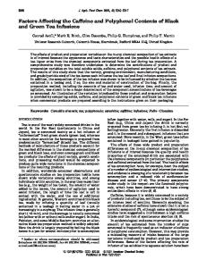
FIG. 8. Schematical top and cross-sectional views of a dielectric with cylindrical pores capped by a thin conductive layer. All pores remain open, so that the electrical current is forced into a smaller conductive cross section.
IV. DISCUSSION
Overall, the measurements indicate that the properties of thin Ta共N兲 layers are strongly dependent on the underlying dielectric substrate. Two main parameters, in particular, related to the substrate play an important role in determining the properties of the thin Ta共N兲 cap layers: morphology and surface composition. A. Influence of morphology FIG. 7. C1s and Si2p emission peaks at about 7 nm sputtering depth 共see Fig. 5兲, before the interface of Ta共N兲/SiC:H is reached: the presence of C is clearly detectable while the Si cannot yet be distinguished from the background.
It can be noticed that while in the case of Ta共N兲/NP1 the profile of Ta appears fairly sharp, with a fast decrease in Ta intensity once it is past the interface 共Fig. 6兲, at the Ta共N兲/ SiC:H interface of the Ta共N兲/SiC:H/P1 sample the decrease in Ta concentration is more gradual 共Fig. 5兲. Another detail that can be noticed in Fig. 6 is that the C1s signal appears in the depth profile significantly earlier than in the interface region. This is also seen in Fig. 7, where the C1s and Si2p spectra recorded at a sputtering depth of about 7 nm are shown: the C1s emission peak is already present, while the Si2p peak 共around 103 eV兲 is not yet distinguishable from the background. Since the inelastic mean free path of the C1s electron is smaller than that from Si2p , this provides indirect indication that interaction has taken place between the Ta共N兲 and SiC:H. Also, the second interface in Fig. 5 共between the SiC:H and the P1 layers兲 is not sharp, especially when looking toward the C profile. This phenomenon can be explained by the fact that some C has diffused into the inorganic porous film during CVD cap deposition.12 Figure 5 also shows that a significant amount of O is incorporated into the thin a-SiC:H cap layer. Amorphous SiC:H layers are generally prone to oxidation once they are exposed to ambient conditions, and this tendency is amplified in a porous film. Finally, when Ta共N兲 is directly deposited on the NP1 the presence of a Ta oxide peak (Ta2 O5 ) was observed at the interface, with intensity comparable to or higher than that of the oxide peak at the top surface of the Ta共N兲 layer 共Fig. 6兲. The Ta oxide peak is not observed at the barrier/dielectric interface when Ta共N兲 is deposited on the intermediate SiC:H layer 共Fig. 5兲.
The morphology of the substrate surface has influence on the degree of uniformity and continuity of the Ta共N兲 layer deposited on top through two main parameters: roughness and porosity at the surface. The strong correlation noticed between substrate roughness and the increase in sheet resistance of Ta共N兲 films on nonporous substrates is attributed to an increase in the effective area to be covered by the PVD deposition, regardless of their composition. For a fixed sputtering time, on top of a substrate with higher roughness, an equal amount of material has to distribute over a larger surface, which leads to a decrease in the thickness deposited. From Table I it can be observed that the surface roughness values before and after the deposition of 10 nm Ta共N兲 are essentially the same, indicating conformal coverage. This correlation does not hold for porous substrates. On the other hand, a clear correlation exists between the sealing performance of the Ta共N兲 layers and sheet resistance values: porous Ta共N兲 cap layers show abnormally high resistance, like samples 5, 6, and 9 in Table I. This can be explained in the following way. We consider a model in which a dielectric film has uniformly distributed cylindrical pores, with porous volume fraction equal to P. If the capping film deposited on top of this surface is thin enough, all pores at the surface will still be open, as shown schematically in Fig. 8. Measuring the sheet resistance of thin films by a four-point probe14 under such conditions would mean that the effective area of the current rings generated in the porous Ta共N兲 would be approximately equal to A eff⫽A(1⫺P), where A is the initial area and P is the porous fraction, transferred from the porous dielectric to the thin conductive film. Substituting A eff in the expression for the calculation of the resistance R by a fourpoint probe system,14 where is the resistivity of the metal, we obtain dR⫽ 共 dx/A eff兲 ⫽ 关 dx/A 共 1⫺ P 兲兴 .
共1兲
Integrating Eq. 共1兲 along distance x between the two four-
Downloaded 05 Sep 2002 to 146.103.254.11. Redistribution subject to AIP license or copyright, see http://ojps.aip.org/japo/japcr.jsp
Iacopi et al.
J. Appl. Phys., Vol. 92, No. 3, 1 August 2002
1553
point probe pins, where the drop in potential is measured, and extracting the sheet resistance from R s ⫽ /t 共t is the conductive film thickness兲, we obtain the following expression: Rs⫽ 兵 / 关共 1⫺ P 兲 ln 2 兴 其 共 V/I 兲 ,
共2兲
where I and V represent the forced current and the measured drop in potential in a four-point probe measurement, respectively. Expression 共2兲 indicates that the measured sheet resistance is 1/(1⫺ P) times higher than that measured on a nonporous conductive film. This of course only holds provided the conductive film thickness is the same, which also means both the porous and the nonporous substrates should have similar surface roughness. This is indeed very close to our situation if one compares the P1 共P⬵0.5, rms⫽0.35 nm兲 to the a-SiC:H 共P⫽0, rms⫽0.35 nm兲. The sheet resistance of a 10 nm Ta共N兲 film on P1 is 455 ⍀/sq, which is about 1.86 times higher than the sheet resistance of an equivalent Ta共N兲 film on an a-SiC:H dielectric. For P⫽0.5 we would obtain 1/(1⫺ P)⫽2, which is reasonably close to 1.8 –1.9. This is probably an extreme case where all pores remain open after Ta共N兲 deposition. The other porous Ta共N兲 in Table I all present significantly lower sheet resistance values than Ta共N兲 on P1, even though the P2 and P3 dielectric substrates present comparable or higher porosity. With regard to this, pore size 共which is on average lower than for P1兲 definitively plays a role: for an equivalent capping layer thickness, smaller pores will be more easily ‘‘bridged.’’
B. Influence of chemical composition
The surface composition of the substrate, together with the thermodynamic conditions, determines whether a chemical reaction can take place between the Ta and the dielectric material. Chemical reactions at the interface could affect the properties of Ta共N兲 thin films. The presence of a Si–O–Si backbone enhances the possibility of oxidation of the Ta at the interface with the dielectric film, as seen in the case of Ta共N兲 on NP1 film. Ta共N兲 oxidation does not occur when the Ta共N兲 layer is deposited on top of an a-SiC:H film 共as seen in Fig. 5兲. Apart from oxidation, no other specific reactions of Ta should be expected on inorganic dielectric substrates like SiO2 , NP1, and P1, as previously reported by other researchers.15 Except for these materials, all the remaining dielectric substrates investigated in this study contain C 关Table I 共1兲兴. By XPS depth profiling on the Ta共N兲/SiC:H/P1 sample, the presence of C in the Ta共N兲 layer was observed, which could point to a reaction at the Ta共N兲/SiC:H interface. In the literature, several references can be found that report the formation of Ta–C bonds at the interface when Ta or Ta共N兲 compounds are deposited on substrates containing carbon,16 due to the high formation enthalpy of the Ta–C bond (⌬ f H 0 (TaC) ⫽⫺34.44 kcal/mol). 17,18 In this XPS study, no evident chemical shifts that directly prove the formation of a TaC compound have been observed. Note, however, that no significant shifts are expected in the Ta4 f emission peak between the –N and the –C bonded Ta.15,16 Furthermore, for both C–Si and C–Ta carbidic bonds, the C1s emission peak
FIG. 9. Mechanism leading to local cross-linking enhancement of dielectric matrices containing CHx functional groups: the presence of TaC crystallites or unreacted Ta, together with the high temperature and ion bombardment from the PVD deposition, result in weakening and eventual breaking of C–H bonds. Crosslinking among two neighboring polymer chains can take place.
is expected in the binding energy range between 282.4 and 283.1 eV.19,20 The fact that the C1s emission peak is detected in the Ta共N兲 region a few nm from the Ta共N兲/SiC:H interface, and that the long Ta tail is observed in the depth profile in Fig. 5 both indicate interaction between the C of the SiC:H and the Ta of the barrier layer. It is possible to identify a correlation between the carbon content at the dielectric surface, on the one hand, and the sealing properties of porous low-k dielectrics by PVD Ta共N兲, on the other hand 共Table I兲. The deposition of 10 nm Ta共N兲 on the P3 film 共with high C concentration兲 yields a fully closed cap layer, while an equivalent Ta共N兲 film, the P2 dielectric 共low C concentration兲, has a higher sheet resistance and appears to still be porous. A remarkable reduction in sheet resistance can be noticed also in the P1 films when capped by 5, 10, or 20 nm a-SiC:H. Moreover, 10 nm Ta共N兲 are efficiently seals the P1 sample precapped by 10 nm SiC:H 共Table I, sample 7兲. When depositing either only Ta共N兲 or only a-SiC:H on a P1 film, about a 30 nm capping thickness is needed to achieve full sealing. This indicates that there is a correlation between the tendency of Ta to react with C and the sealing efficiency. In order to explain the beneficial influence of the presence of surface C on the pore sealing properties of PVD Ta共N兲 depositions, the following mechanism is proposed. The tendency of sputtered Ta atoms to react with C at the surface of the dielectric can lead to the formation of Ta–C.16 Because of this, the wetting capability of Ta共N兲 on the dielectric surface is enhanced and structural rearrangement of the bonds/charges takes place in the top layers of the dielectric matrix. At the interface between the dielectric and the Ta共N兲 film, a ‘‘transition layer’’ with high intermixing forms. A considerable number of Ta atoms are dispersed in the initial matrix 共a-SiC:H for the capped P1 or siloxane for the P2 and P3兲, either unreacted or in the form of Ta–C crystallites. Under these conditions, already reported by Gerstenberg and Grischke,17 the pristine carbidic bonds in the dielectric matrices 共mainly C–Hx like, since the covalent Si–C bonds are much stronger兲 are weakened, due to charge delocalization effects induced by the presence of neighboring metal atoms. Moreover, the high deposition temperature and the ion bombardment energy released during the PVD deposition further favor the breaking of these bonds, and can lead to crosslinking of the top layers of the matrix through the formation of a C–C bond across the polymer chains,17 like schematically shown in Fig. 9.
Downloaded 05 Sep 2002 to 146.103.254.11. Redistribution subject to AIP license or copyright, see http://ojps.aip.org/japo/japcr.jsp
1554
Iacopi et al.
J. Appl. Phys., Vol. 92, No. 3, 1 August 2002
In this study we have focused on amourphous SiC:H and organic-doped silicate glasses, but the mechanism reported can also be extended to other classes of dielectrics and allow matrix cross-linking effects, like organic polymers. In addition, from the point of view of the metallic barrier material, not only Ta but also other metals could lead to a similar effect, provided that their respective carbidic bonds exhibit a high formation enthalpy 共i.e., ⌬ f H 0 (TiC)⫽⫺44 kcal/mol and ⌬ f H 0 (ZrC)⫽⫺47 kcal/mol兲.18 V. CONCLUSIONS
In this article the dominant mechanisms for sealing porous substrates by PVD thin film deposition were investigated. The porous substrates were selected, on the one hand, for their different morphological characteristics, i.e., surface roughness, porosity, and average pore size and, on the other hand, for their chemical compositions. Significantly thicker Ta共N兲 layers are required in order to obtain a fully closed cap layer on top of mesoporous low-k films compared to nonporous dielectrics, as indicated by sheet resistance and ellipsometric porosimetry measurements. The sealing efficiency of thin Ta共N兲 barrier layers depends not only on the porosity and pore size but also on the surface composition of the dielectrics. In particular, a strong correlation was observed between the C content of the substrate and the sealing performance of PVD Ta共N兲 films on porous low-k films. Higher C concentrations lead to faster sealing of the pores in conditions of similar pore size and porosity. The model proposed to explain the mechanism is based on the formation of a transition layer at the Ta共N兲/ dielectric interface where Ta acts as a ‘‘catalyst’’ that locally promotes crosslinking of the matrix. ACKNOWLEDGMENTS
The authors acknowledge the Dow Corning Corporation, in particular Ben Zhong and the researchers in the IMEC– Dow Corning affiliation program: Herman Meynen, Ken Weidner, and Ste´phane Malhouitre. Danielle Vanhaeren is gratefully acknowledged for AFM measurements, as is Youssef Travaly for valuable discussions. The ERDA project was supported by the Fund for Scientific Research Flanders
共Belgium兲 Grant No. FWO42/476 and as an EC program ‘‘Access to Research Infrastructure Grant No. EU/HPRI-CT1998-00039.’’ International Technology Roadmap for Semiconductors 共ITRS兲, Semicond. Industry Asso., update 2001. 2 S. P. Murarka, Mater. Sci. Eng., R. 19, 87 共1997兲. 3 Y. Shacham-Diamand and A. Dedhia, J. Electrochem. Soc. 140, 2427 共1993兲; F. Lanckmans, L. Geenen, S. Arnauts, W. Vandervorst, and K. Maex, J. Vac. Sci. Technol. B 共to be published兲. 4 J.-N. Sun, D. W. Gidley, T. L. Dull, W. E. Frieze, A. F. Yee, E. T. Ryan, S. Lin, and J. Wetzel, J. Appl. Phys. 89, 5138 共2001兲. 5 F. Iacopi, Zs. To¨kei, D. Shamiryan, Q. T. Le, S. Malhouitre, M. Van Hove, and K. Maex, Proceedings of the Advanced Metallization Conference 共AMC兲, 9–11 October 2001, Montre´al, Canada. 6 D. Shamiryan, M. R. Baklanov, Zs. To¨kei, F. Iacopi, and K. Maex, in Ref. 5. 7 Zs. To¨kei, J. J. Waeterloos, F. Iacopi, R. Caluwaerts, H. Struyf, J. Van Aelst, and K. Maex, in Ref. 5. 8 M. J. Loboda and G. A. Toskey, Solid State Technol. 41, 99 共1998兲; M. G. Albrecht and C. Blanchette, J. Electrochem. Soc. 145, 4019 共1998兲. 9 S. Moyer, K. Chung, M. Spaulding, T. Deis, R. Boisvert, C. Saha, and J. Bremmer, Proceedings of the International Interconnects Technology Conference 共IITC兲, 1999, pp. 196 –197; R. A. Donaton et al., International Interconnects Technology Conference 共IITC兲, 2000, p. 93; C. Jin and J. Wetzel, ibid., p. 99; F. Iacopi et al., Proceedings of the Advanced Metallization Conference (AMC) 2000 共Materials Research Society Pittsburgh, 2001兲, pp. 287–299. 10 F. N. Dultsev and M. R. Baklanov, Electrochem. Solid-State Lett. 2, 192 共1999兲; M. R. Baklanov, K. P. Mogilnikov, V. G. Polovinkin, and F. N. Dultsev, J. Vac. Sci. Technol. B 18, 1385 共2000兲. 11 U. Kreissig, S. Grigull, K. Lange, P. Nitzsche, and B. Schmidt, Nucl. Instrum. Methods Phys. Res. B 138, 674 共1998兲. 12 F. Iacopi, M. R. Baklanov, E. Sleeckx, T. Conard, H. Bender, H. Meynen, and K. Maex, J. Vac. Sci. Technol. B 20, 109 共2002兲. 13 K. P. Mogilnikov 共private communications兲. 14 F. M. Smits, Bell Syst. Tech. J. 37, 371 共1958兲. 15 Y. Zeng, S. W. Russell, A. J. McKerrow, L. Chen, and T. L. Alford, J. Vac. Sci. Technol. B 18, 221 共2000兲. 16 G. R. Yang, Y. P. Zhao, B. Wang, E. Barnat, J. McDonald, and T. M. Lu, Appl. Phys. Lett. 72, 1846 共1998兲; J. W. Nah, W. S. Choi, S. K. Hwang, and C. M. Lee, Surf. Coat. Technol. 123, 1 共2000兲; T. Hara, K. Sakamoto, F. Togoh, H. Yang, and D. R. Evans, Jpn. J. Appl. Phys., Part 2 39, L506 共2000兲; J. Kelber, in Ref. 5. 17 K. W. Gerstenberg and M. Grischke, J. Appl. Phys. 69, 736 共1991兲. 18 National Institute of Standards and Technology, Standard Reference Data Program 共2001兲. 19 M. H. Tsai, S. C. Sun, H. T. Chiu, C. E. Tsai, and S. H. Chuang, Appl. Phys. Lett. 67, 1128 共1995兲. 20 R. Teghil, L. D’Alessio, M. Zaccagnino, D. Ferro, V. Marotta, and G. De Maria, Appl. Surf. Sci. 173, 233 共2001兲; R. Teghil, L. D’Alessio, G. De Maria, and D. Ferro, ibid. 86, 190 共1995兲. 1
Downloaded 05 Sep 2002 to 146.103.254.11. Redistribution subject to AIP license or copyright, see http://ojps.aip.org/japo/japcr.jsp