720
IEEE TRANSACTIONS ON DEVICE AND MATERIALS RELIABILITY, VOL. 5, NO. 4, DECEMBER 2005
Ferroelectric Polymer Langmuir–Blodgett Films for Nonvolatile Memory Applications Stephen Ducharme, Member, IEEE, Timothy J. Reece, Christina M. Othon, and R. K. Rannow, Member, IEEE
Abstract—We review the potential for integrating ferroelectric polymer Langmuir–Blodgett (LB) films with semiconductor technology to produce nonvolatile ferroelectric random-access memory (NV-FRAM or NV-FeRAM) and data-storage devices. The prototype material is a copolymer consisting of 70% vinylidene fluoride (VDF) and 30% trifluoroethylene (TrFE), or P(VDF-TrFE 70:30). Recent work with LB films and more conventional solventformed films shows that the VDF copolymers are promising materials for nonvolatile memory applications. The prototype device is the metal–ferroelectric–insulator–semiconductor (MFIS) capacitance memory. Field-effect transistor (FET)-based devices are also discussed. The LB films afford devices with low-voltage operation, but there are two important technical hurdles that must be surmounted. First, an appropriate method must be found to control switching dynamics in the LB copolymer films. Second, the LB technology must be scaled up and incorporated into the semiconductor-manufacturing process, but since there is no precedent for mass production of LB films, it is difficult to project how long this will take. Index Terms—Ferroelectric memory, ferroelectric polymer, Langmuir–Blodgett (LB) films, nonvolatile memory.
I. I NTRODUCTION
D
UE to the proliferation of portable computing, information management, and communications devices, there is a large and growing demand for technologies enabling the rapid manipulation, caching, and storage of large amounts of data. Many of these applications put a premium on convenience, speed, energy efficiency, affordability, and reliability. There are several current technologies providing some form of nonvolatile random-access-memory (NV-RAM) data storage to meet these needs. Currently, the most widely used nonvolatile NV-RAM technology is Flash, a charge-storage technology that can achieve relatively high density at low cost because it is based on standard silicon integrated-circuit technology. The main drawbacks of Flash memories are low speed, cycle energy usage, and limited cycle life. Other candidate NV-RAM technologies currently under consideration include magnetic (MRAM), phase change (OUM), resistive (RRAM), and ferroelectric (FRAM) [1]. Manuscript received February 26, 2005; revised July 27, 2005. This work was supported by the Nebraska Research Initiative, the National Science Foundation, and the Office of Naval Research. S. Ducharme, T. J. Reece, and C. M. Othon are with the Department of Physics and Astronomy and the Center for Materials Research and Analysis, University of Nebraska, Lincoln, NE 68588-0111 USA (e-mail: sducharme1@ unl.edu). R. K. Rannow is with Hewlett-Packard Corporation, Corvallis, OR 973304239 USA. Digital Object Identifier 10.1109/TDMR.2005.860818
A. Ferroelectric Memories A ferroelectric crystal maintains a permanent electric polarization that can be repeatably switched between two stable states by an external electric field [2], [3], thus exhibiting a polarization–electric-field-hysteresis loop, analogous to the magnetization–magnetic-field-hysteresis loop exhibited by ferromagnetic crystals. In addition, like magnetic materials, ferroelectric crystals can form domains, each with a unique polarization axis. The hysteresis loops are characterized by the magnitude of the zero-field remanent polarization after saturation with a large electric field and by the magnitude of the coercive field EC , the minimum value of the electric field necessary to reverse, or switch, the polarization state. The essential bistability of ferroelectric polarization in a thin film can be exploited to make a nonvolatile memory, a small but rapidly growing FRAM technology finding its way into, e.g., smart cards and cache chips [4]–[6]. The available devices are based on perovskite ferroelectrics such as lead zirconium titanate (PZT) or strontium barium titanate (SBT). In developing commercially viable devices, researchers overcame many difficult hurdles, most notably film degradation (“fatigue”) after repeated switching due to chemical instabilities in the films and at the interfaces [6]–[10]. Another drawback is that perovskites generally require high-temperature annealing that is harmful to other components on the chip. Though new formulations should reduce the annealing temperature significantly to improve compatibility, the perovskite memory chips still require buffer layers and complex mask sets [11]–[17]. Ferroelectric memories in current use employ a destructive-readout scheme, because leakage tends to quickly shield the polarization field [6]. Even with destructive readout, FRAMs are faster and use much less energy than other technologies in current use. For example, current read-and-write operations in perovskite FRAMs take approximately 1 µs, use approximately 1 nJ per bit, and the devices can be useful for 1010 cycles or more. In contrast, current technologies are much slower and require much more energy. For example, electrically erasable programmable readonly memory (EEPROM) requires 10 µs and 1 µJ to write a bit, and Flash requires 500 µs and 2 µJ but last only about 106 cycles [4]. There is much current research into metal– ferroelectric–insulator–semiconductor (MFIS) bistable capacitors and ferroelectric-field-effect-transistor (Fe-FET) devices, which add a source and a drain to the MFIS configuration to permit nondestructive readout. The MFIS and Fe-FET memory devices generally have short data-retention times due to leakage, depolarization, or both [18], [19], though some specific examples have shown retention times of days [20], [21]. This
1530-4388/$20.00 © 2005 IEEE
DUCHARME et al.: FERROELECTRIC POLYMER LB FILMS FOR NONVOLATILE MEMORY APPLICATIONS
is long enough for many applications, where data can be occasionally refreshed through pulsed (destructive) readout and rewriting. One promising material class for use in nonvolatile memories is ferroelectric vinylidene-fluoride (VDF) polymers, such as polyvinylidene fluoride (PVDF), [C2 H2 F2 ]n , and its copolymers with trifluoroethylene (TrFE), [(C2 H2 F2 )x (C2 HF3 )1−x ]n , or with other monomers [22], [23]. The VDF copolymers have a large spontaneous polarization ∼ 0.1 C/m2 [24], [25], excellent polarization stability, and switching times as short as 0.1 µs [26], [27]. Their high resistivity of up to 1000 TΩ · cm means low leakage, suitable for fabrication of Fe-FETs. Further, they do not require high-temperature processing, have outstanding chemical stability and low fabrication costs, and are nontoxic. Besides current development efforts to commercialize simple cross-point destructive-readout memories [1], [28], there have been encouraging laboratory demonstrations of memory elements incorporating VDF copolymers [29]–[34], as described in Section III. B. Ferroelectric Polymers Both piezoelectricity and pyroelectricity were observed over 30 years ago in PVDF. Piezoelectric transducers made by solvent casting were soon commercially available, though it took a decade to establish that ferroelectricity was the origin of these effects in PVDF [35]. Synthesis of PVDF and its copolymers has been standardized [36], [37] and is thoroughly described in the texts edited by Wang et al. [38] and Nalwa [39], and in several review articles [22], [40]–[42]. PVDF is the most widely used ferroelectric polymer and is manufactured in large quantities for a wide variety of applications, ranging from protective coatings to ultrasound transducers. The materials are available in pellet or powder form and require no special precautions for handling and storage. Modern polymer synthesis and processing technology is more than adequate for the task of producing high-purity materials with well-defined molecular-weight distribution. Though PVDF shows clear repeatable polarization hysteresis, there was doubt initially that this was of ferroelectric origin because many polymers exhibit long-lived but transient hysteresis due to either charge injection or induced polarization. Either of these mechanisms produces electrets, which exhibit metastable piezoelectric and pyroelectric effects that can persist for hours, days, or even years. Direct evidence of ferroelectricity was first provided by X-ray diffraction studies [35] and unambiguous evidence that hysteresis was due to switching between opposing but equivalent polarization states came from the synthesis and systematic study of the copolymers with TrFE [23] and tetrafluoroetylene (TeFE) [43]. The substitution of either TrFE or TeFE suppresses the ferroelectric–paraelectric phase-transition temperature below the melting point, thus providing a direct connection between the switching charge and the appearance of spontaneous polarization [44]. The molecular units in the polymer chains of PVDF and P(VDF-TrFE) have net dipole moments pointing from the electronegative fluorine to the electropositive hydrogen, as shown in Fig. 1(a). These chains can crystallize in parallel rows
721
Fig. 1. Structure of the PVDF and its copolymers. (a) Structure of the all-trans conformation showing the planer carbon backbone with attached fluorine and hydrogen atoms; (b) crystal structure of the ferroelectric β phase, where the all-trans polymer chains are viewed end-on, showing the quasi-hexagonal close packing of the polymer chains.
[Fig. 1(b)] and, in the ferroelectric state, the dipoles of all chains are aligned along a twofold crystalline axis, resulting in a macroscopic polarization. Switching is accomplished by applying a large electric field opposing the polarization. The main advantages of ferroelectric polymers relative to perovskites are the low production costs, ease and flexibility of fabrication in a variety of thin-film forms, chemical stability, and resistance to degradation caused by strain or defects. The disadvantages of the polymers relative to perovskites are their relatively low melting point (150 ◦ C–200 ◦ C), low stiffness, and the polymorphous structure of solvent-formed samples. Ferroelectric polymer samples are typically prepared by solvent methods because they do not crystallize well from the melt [38]. The polymer is first dissolved in a polar solvent at concentrations of a few weight percent. The solution is then formed into sheets or films by casting or spinning and the solvent evaporated, leaving a pliable solid sample that is typically polymorphous—an inhomogeneous mixture of amorphous and crystalline material. The crystallites can have multiple structures and usually have lamellar morphology with dimensions of order 50 nm × 500 nm × 5 µm, with the chains parallel to the shortest dimension, folding back and forth. The lamellae are microscopically ferroelectric, with in-plane polarization. To improve crystallinity and produce macroscopic polarization, the polymorphous samples are heated and drawn to ratios of 3:1 or more and poled by applying a large voltage across the film or sheet. By these means, it is generally possible to obtain ∼ 50% crystallinity and ∼ 25% polarization with PVDF and over 90% crystallinity and 80% polarization with copolymers containing approximately 50%–80% VDF [41]. About 10 years ago, the group at Yamagata University developed techniques for producing essentially 100%-crystallinity optically clear, though highly twinned, crystals several-hundred micrometers thick [45], [46], an impressive achievement. Another notable innovation by a group at Kyoto University is the growth by epitaxial vapor deposition of crystalline mats of VDF oligomers consisting of short iodine-terminated chains of VDF with the chemical formula CF3 −[CH2 − CF2 ]17 −I [47], [48]. The oligomer films are likely ferroelectric as they exhibit reversible switching. The oligomer films are promising alternatives to PVDF or its copolymers, but relatively little is known about their behavior. The oligomers are appealing for
722
IEEE TRANSACTIONS ON DEVICE AND MATERIALS RELIABILITY, VOL. 5, NO. 4, DECEMBER 2005
Fig. 2. Horizontal (Schaefer) LB deposition by putting the substrate in contact at a slight angle to the surface Langmuir layer on the water trough [54].
several reasons. 1) They have the same basic conformational structure as PVDF. 2) They are easily deposited by evaporation. 3) They may be amenable to Langmuir–Blodgett (LB) deposition because the chain lengths and the terminating groups, CF3 and I, can be changed to control film-forming properties and functionality. 4) As monodispersed molecules, they crystallize more readily and should have fewer chain-folding defects and lamellar structures than those that are prevalent in PVDF and its copolymers. 5) They have sustained reversible polarization patterns with dimensions of 65 nm or smaller. 6) The chain ends may constitute natural nucleation sites, increasing nucleation rates for faster switching, as propagation distances would be only 5 nm. They should be able to reach very-high bit densities as demonstrated in atomic-force-microscopy (AFM) studies of rewritable bits as small as 65 nm [49]. C. LB Films The LB technique is a means of depositing uniform molecular monolayers (MLs) on solid substrates. It exploits the ability of some substances to form a very thin, typically monomolecular, layer on the surface of a liquid subphase, usually water. This Langmuir layer may be transferred onto a substrate by vertical dipping or, less often, by horizontal transfer, as shown in Fig. 2. Repeating the transfer process, one builds up an LB film, whose thickness is precisely determined by the thickness of a single layer and the number of transfers. The ability to control the film thickness on a molecular level is the most prominent feature of the technique. Another important feature is the ability to control film structure by adjusting conditions on the liquid subphase, which is usually bounded by air or an inert atmosphere, before transfer to a solid substrate. Trough conditions affecting film formation include dispersal solvent and method, compression rate, compression history, surface pressure, subphase temperature, subphase composition and pH, deposition angle, and deposition rate. There are several comprehensive monographs reviewing the fabrication and applications of LB films [50], [51]. The LB technique was initially developed for the deposition of monomolecular layers of fatty acids because these materials are strong amphiphiles, which have a polar “head” that is soluble in a polar subphase (e.g., water), and an alkyl tail, which is not soluble. The amphiphilic character of the molecules confines them to the surface, forming a robust monomolec-
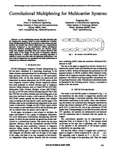
Fig. 3.
Pressure–area isotherm of P(VDF-TrFE 70:30) recorded at 25 ◦ C.
ular Langmuir layer. The LB technique can also be used with large molecules, such as polymers, with slow dissolution kinetics in the subphase. LB films of polymers have received relatively little attention, but are mentioned in two popular monographs [50], [51], and discussed in more detail in two reviews [52], [53]. Even though PVDF and its copolymers are not good amphiphiles, it turns out that they can be dispersed on top of the water subphase to form a sufficiently stable Langmuir layer, with a repeatable pressure–area isotherm, like the one shown in Fig. 3. Because of the solubility, dispersal can be inefficient; up to 90% of the dispersed polymer can be taken up in water. Also, the Langmuir layer is only metastable as it slowly dissolves in water, but this takes weeks, and so is not a significant impediment to LB deposition. PVDF and related polymers are not very soluble in volatile and water-immiscible solvents, such as chloroform and hexane, which are frequently used in LB deposition. They are soluble in polar solvents, such as acetone and dimethyl sulfoxide (DMSO), which are miscible with water and carry much of the polymer into the water solution, reducing the efficiency of film dispersal; only about 10% of the polymer remains on the surface. Good ML and multilayer films can be prepared using the standard vertical-dipping method, or by horizontal dipping (Fig. 2). The ferroelectric copolymer-LB films are prepared as follows. A solution of the copolymer, with a concentration of about 0.05 wt.% in either acetone or DMSO, is dispersed in 50-µL drops from a pipette at a rate of 2–4/min onto an ultrapure (18 MΩ · cm) water subphase at or near room temperature. Approximately 1 mL of solution (about 0.5 mg of polymer) is required to fill 500 cm2 of trough area. The surface layer is then compressed by closing perimeter barriers slowly until a working pressure of 5 mN/m is reached. The film should have a smooth and nonhysteretic pressure–area isotherm like that shown in Fig. 3. Deposition is best done by lowering the substrate nearly horizontally to the surface layer, as shown in Fig. 2. Additional details on fabrication are given elsewhere [54], [55]. The LB method produces highly planar ordered films, as shown in the scanning-tunneling-microscopy (STM) image in
DUCHARME et al.: FERROELECTRIC POLYMER LB FILMS FOR NONVOLATILE MEMORY APPLICATIONS
723
Fig. 4. Structure of ferroelectric polymer LB films. (a) STM image of a 1-ML film on graphite [56]; (b) chain orientation and stacking in a multilayer sample. The arrows represent the CF2 −CH2 dipole moments and the zigzag lines the all-trans carbon backbone.
Fig. 5. Two measures of thickness for the copolymer-LB films [62], [64]. (a) LB-film thickness; (b) reciprocal capacitance per unit area versus number of layers for 70:30 copolymers deposited on a silicon wafer.
Fig. 4(a) [56]. By repeated deposition, we obtain multilayers with the chains laying parallel to the surface, as shown in Fig. 4(b) and verified by theta-2-theta X-ray diffraction, which measures the (110) close-packing peak perpendicular to the layers [57]–[61]. This means that the polarization, which is along the (010) direction [57], is tilted about the chain axis 30◦ away from the film normal. The films then are crystalline mosaics, having uniform orientation normal to the substrate, but with disordered in-plane orientation [62]. The films often require thermal annealing in the paraelectric phase (100 ◦ C–150 ◦ C for the 70:30 copolymer), with best results from annealing close to, but below, the melting point [62], [63]. Because the polymer is not a good amphiphile, and therefore the film on the trough is not a true ML, it tends to produce films somewhat thicker per nominal ML, about two to three times the molecular diameter for PVDF copolymers [62]. We calibrated film thickness with variable-angle spectroscopic ellipsometry (VASE, J. A. Woollam Company) using a pie-shaped sample on a 3-inch silicon wafer. Multisample analysis allows the independent determination of substrate and film optical constants and film thickness. As shown in Fig. 5(a), the thickness of the LB films of the 70:30 copolymer-LB films deposited at 5-mN/m pressure and 25 ◦ C temperature is linear in the number of MLs, with an average thickness of 1.78 ± 0.07 nm, about three times the molecular diameter [62], [64]. Capacitance measurements [Fig. 5(b)] on another series of films deposited on glass with aluminum electrodes returned a dielectric constant of 9.9 ± 0.4, consistent with bulk values [42].
Though our methods for depositing the copolymer-LB films result in consistent ferroelectric properties, characterization results suggest that there is considerable room for improvement. Some properties are highly consistent and relatively insensitive to deposition conditions, such as transition temperature, polarization hysteresis, and film capacitance. But several other properties are much more sensitive to deposition conditions, such as dc and ac conductance, crystallinity, and switching kinetics. Closer examination of film morphology by electron microscopy and scanning-probe microscopy reveals considerable variation, probably connected with the process of film formation on the trough and during film transfer to the substrate. This will be more critical as the device size is reduced. Film annealing might also be improved, but cannot make up for poor morphology— the individual MLs must be highly planar to begin with. The LB deposition technique is fundamentally scalable to any desired area. The main challenges are logistical, as after each ML transfer, either the wafer or the surface layer must be translated and the surface-layer pressure reestablished. For this reason and for improved control of the transfer process, it may be best to use vertical transfer so that the film can be continuously fed to the substrate. LB deposition has become a sophisticated research tool, and several companies sell turn-key LB systems for laboratory use. These systems are generally capable of handling wafers of 3–6 in and are readily scaled up to larger wafers. There is no serious impediment to scaling LB deposition for manufacturing, as the water surface area is virtually unlimited. To our knowledge, there has been no
724
IEEE TRANSACTIONS ON DEVICE AND MATERIALS RELIABILITY, VOL. 5, NO. 4, DECEMBER 2005
use of LB deposition in mass production, though some small companies make custom thin films, mainly for research and development purposes or for low-volume applications. There are, however, several practical matters connected with mass production that need attention. The major challenge posed by LB manufacturing is not trough capacity, but film replenishment. For example, a 6-inch wafer requires nearly 200 cm2 of new film per deposited layer. It is straightforward to use a series of independent LB troughs and cycle the wafers among them, so that some troughs are in use while others are replenished. Going beyond this, Barroud and Vandevyver [65] developed a clever method for continuous replenishment using a two-section trough separated by a suitable hydrophobic cylinder. The material is continuously dispersed at low surface pressure (i.e., a two-dimensional gas phase) into one section and rolls onto the cylinder, which transfers it to the second section, compressing the layer to a two-dimensional liquid or solid phase as it flows, much like a vapor compressor for three-dimensional compression. This type of system can be operated indefinitely, with proper process control. Another challenge is to keep the water sufficiently still. The surface does not need to be optically flat, but ripples can distort the film on the trough and, more critically, at the transfer meniscus. A number of techniques can be used to quiet the water. Passive methods include providing vibration and acoustic isolation and using shallow troughs with contoured bottoms and submerged baffles designed to damp or disperse ripples. Active methods include actively controlled buffer barriers that can be segmented to control the surface modes of the trough. It is also necessary to control subphase pH and temperature and to replenish and keep the subphase clean. These are all readily done with proper process-control systems. Standard clean-room conditions should be adequate for the LB system. There is no need for atmosphere passivation because the copolymers are chemically inert, though an inert atmosphere of, e.g., nitrogen, might be beneficial. LB deposition of the copolymers will entail relatively little environmental hazard. The most abundant substance in the process is water. The copolymers are nontoxic, and being chemically very similar to Teflon-PVDF, is Food and Drug Administration (FDA) approved. The small amount of solvent used for dispersal is easily recovered as it evaporates from the trough surface. Even with a relatively poor loading efficiency, we use about 1–2 mL of solvent per 1000 cm2 of dispersed film. For devices composed of 20-ML LB films, this translates to 20–40 mL per 1000 cm2 of trough area. Improvements in loading efficiency could reduce solvent use by up to 90%. II. T WO -D IMENSIONAL F ERROELECTRIC P OLYMERS The first LB films of the VDF copolymers were made in Moscow in 1995 [66], [67]. The nanometer thickness and high quality of the LB films have led to a number of notable achievements: the discovery of two-dimensional ferroelectricity [56]; discovery of a bulk stiffening transition [68]; the first direct measurement of the intrinsic ferroelectric coercive field [69] and the first measurement of intrinsic switching kinetics [70].
Two comprehensive reviews describe these results in detail [54], [60], and an abbreviated review [71] summarizes the essential physics of the films. A. Film Structure Film morphology is readily probed by scanning electron microscopy (SEM), AFM, STM, optical microscopy, and optical interference profilometry. These studies show that the films are predominately planar, except that about approximately 5% of the surface consists of “tectonic” ridges several micrometers across that appear to be a result of compression stresses that cause local collapse [60], [63]. Since we routinely use electrodes with ≥ 1-mm2 area, these ridges have a minimal effect on measurements. The ridges are a concern for integrated device applications, as they will result in a significant number of failed devices. The STM images [see Fig. 4(a)] [56], [72], [73] often reveal highly planar and ordered arrays of straight polymer chains, but these images are not necessarily representative. The copolymer-LB films have uniformly good crystallinity after annealing, with the chains flat against the substrate and (110) crystal orientation, as shown by X-ray diffraction [57] and neutron-diffraction [68] studies. Studies using low-energy electron diffraction (LEED) [73] confirm considerable in-surface order on length scales up to 1 mm, though spectroscopic ellipsometry [74], shows little in-plane anisotropy for the film as a whole, suggesting that the films consist of crystalline mosaics, with a distribution of in-plane orientations. The LB films melt at about 150 ◦ C and only partially recrystallize once melted [63], just like the bulk material. B. Ferroelectric Properties of the Copolymer-LB Films The bistable nature of the copolymer is evident in the hysteresis loops (Fig. 6) recorded using pyroelectric and piezoelectric techniques [75], which show a remarkably large coercive field [69]. The polarization state is stable for at least one year. The films exhibit key features of the first-order ferroelectric–paraelectric phase transition, such as, thermal hysteresis [66], phase coexistence [59], [61], and a linear increase of the phase-transition temperature TC with an applied field [61], [76]. C. Switching Dynamics Extrinsic switching, a process of domain nucleation and growth, has been identified as the dominant switching mechanism in ferroelectric thin films from the earliest studies. It is an activated process characterized by an exponential increase in switching rate (reciprocal switching time 1/τ ) with increased temperature T and electric field E according to the empirically determined form (in the nucleation-limited case) determined by Merz [77]–[79] � � ( c + b) 1 ∝ exp − T (1) τ E
DUCHARME et al.: FERROELECTRIC POLYMER LB FILMS FOR NONVOLATILE MEMORY APPLICATIONS
725
Fig. 6. Hysteresis loops in the piezoelectric and pyroelectric responses in a 30-ML film of P(VDF-TrFE 70:30) as the electric field is cycled around the polarization hysteresis loop [75].
where b and c are constants. Though variations on this exponential form have been reported—such as in the domainwall limited regime—a strong dependence on both temperature and field is almost always observed. Strictly speaking, extrinsic switching does not have a true threshold coercive field because the activation of nucleation permits switching at arbitrarily small fields, but switching experiments are typically carried out with pulses or an ac voltage and so the apparent coercive field is actually a function of pulse duration or ac frequency [80]. Extrinsic coercive fields of most ferroelectrics, typically measured at 50–60 Hz, are in the range 0.01 to 10 MV/m [81]. Coercive fields in thin films generally follow an approximately 2/3 power-law dependence on thickness, which is variously attributed to scaling of nucleation rates or domainwall velocities or some combination of these [82]–[84]. Thin films of PVDF and its copolymers made by solvent methods have coercive fields up to 50 MV/m [85], while LB films have coercive fields up to 500 MV/m [69]. Estimates of the switching time in the VDF copolymers consider the molecular dynamics of the polymer chains. Though the switching of individual polymer chains can be very quick, the propagation of a coherent domain wall requires long-range cooperation that is much more sluggish. The velocity of domain walls propagating is estimated to be 10 m/s for fields of 100 MV/m [86], so crystallites 100-nm wide would switch in 10 ns. The switching studies of Furukawa et al. [26] obtained switching times of ∼ 100 ns with a field of 300 MV/m with solvent-formed films of lamellar crystals. Assuming the domain walls propagated across the lamellae, which typically range from 50 to 500 nm across, this translates into a domain-wall velocity of order 0.5 to 5 m/s. In comparison, the fast switching time of an eight-ML LB film [Fig. 7(b)] was 1.5 µs at 5 V [71], but the crystallite size in the film plane is unknown. The very slow switching observed in many of the thinnest LB films [56], [69], [70], [87] presents a major impediment to NV-RAM applications. Reduction of film thickness may be inhibiting nucleation and domain growth, resulting in higher coercive fields and dramatically slower switching. If the process
Fig. 7. (a) Slow intrinsic switching in a 30-ML film with a high coercive field [71]. (b) Fast intrinsic switching in an eight-ML film with a low coercive field [71].
is nucleation limited, the obvious solution would be to introduce nucleation into these films by the time-honored technique of defect creation. Our preliminary work showed that this can be done through control of fabrication conditions. Fig. 7(a) shows a typical switching transient from a slow intrinsic LB copolymer film [71]. The initial peak at t = 0 is the “RC” discharge current from the capacitor. The second peak superimposed on the capacitor discharge is the polarization switching current. By convention [6], the switching time τ is the time of peak current, which is about 10 s in this example. Most films 30 ML or thinner made on Al-coated glass substrates with Al top electrodes exhibit high coercive field and low-speed switching like this. We found that some of the films made on Al-coated Si substrates, and transferred under slightly different conditions, switched with a much lower field and ten million times faster, as shown in Fig. 7(b) [71]. This is likely due to the reintroduction of nucleation and/or reduction of domainwall pinning. The switched polarization in this case was only 13 mC/m2 , about 8%–9% of the remanent polarization. A test of one sample found that the switched charge degrades by less than 20% after 15 billion cycles. We have also made samples with 25% to 50% switchable polarization, for switching times of about a millisecond. We have concluded that the way to reliable and complete fast switching is to introduce defects to promote nucleation as was likely done in the deposition of the LB films on Al/Si substrates. Defects can come in the form of grain boundaries, local strain, chain folding, chain ends, broken or cross-linked chains, or from impurities. Defects can be introduced by several methods including the following: variation of deposition conditions, polymer modification, variation of film-annealing conditions,
726
IEEE TRANSACTIONS ON DEVICE AND MATERIALS RELIABILITY, VOL. 5, NO. 4, DECEMBER 2005
edge, so the switching time will be limited by the domain-wall velocity. Choosing a conservative velocity of 1 m/s, this would mean a switching time of 100 ns for 100-nm crystallites. Patterning of continuous films can be accomplished by a variety of techniques, such as localized heating, chemical modification, and the creation of physical defect structures by etching or ion implementation in the film, electrode, or substrate. Pattern geometry and scale should influence switching speed, coercive voltage, write energy, and retention. By controlling bit size and shape, switching performance can be better controlled. Patterning should also reduce or eliminate crosstalk between bits. Another means of controlling nucleation and domain motion is synthetic manipulation. By selectively incorporating molecular units or blocks, we can break up the chains and promote nucleation. Similar techniques are currently being investigated with VDF co- and terpolymers to produce relaxor behavior without irradiation [94]. The encouraging results with VDF oligomers [47]–[49], also suggest that chain-end nucleation can be controlled by this means. Fig. 8. (a) Patterned-domain bit. (b) AFM image of ferroelectric nanomesas on a silicon wafer [93]. The diagram shows typical nanomesa dimensions.
doping by atomic and molecular species, irradiation, and film patterning. Irradiation is one way to introduce nucleation defects. Electron irradiation of PVDF copolymers is a common technique used to modify the switching properties [88] or convert them into relaxors [89]. Electron irradiation introduces defects in the form of double bonds and crosslinking, reducing crystallinity and lattice strain. Samples irradiated with dosages of 60–80 Mrad result in materials of the highest electrostriction [90]. For high electron dosages, the samples may be modeled as ferroelectric nanocrystals embedded in an amorphous matrix. It may be that for low dosages the defects may act as nucleation centers to promote switching. However, our studies on LB films and those of other groups indicate that the primary effect of electron irradiation is the conversion of material to an amorphous state, and any increase in switching speed is negligible compared to the loss of crystallinity [91], [92]. Nanoscale patterning can also be used to control nucleation and domain dynamics. Detailed studies of nucleation in ferroelectrics reveal that nucleation almost invariably occurs at defects or crystal boundaries. With the ferroelectric polymer LB films, most or all domain-wall motion will be in the film plane and so the relevant boundaries are lines. By defining planar nanostructures, we should be able to control the precise location of nucleation and the direction of domain-wall motion so that switching becomes more deterministic. For example, a bit composed of nine independent ferroelectric domains is depicted in Fig. 8(a). The total surface charge is proportional to the number and size of the domains. However, the switching time decreases with increasing domain size. Alternatively, arrays of ferroelectric nanomesas 100 nm in diameter and 10-nm thick may be formed by annealing LB films of one to three MLs [93], as show in Fig. 8(b). Because of the highly anisotropic structure of the copolymer lattice, we expect nucleation to take place on one edge and propagate to the opposite
III. I NTEGRATED F ERROELECTRIC P OLYMER D EVICES Ferroelectric polymers based on PVDF are a potential replacement for ferroelectric perovskites currently used in nonvolatile memory elements. Polymers offer the following appealing features. They can be deposited on a wide range of substrates (epitaxy is not necessary), so that they are easily integrated into semiconductor devices. They have low synthesis and fabrication costs. They can be deposited and processed at temperatures below 200 ◦ C and at ambient pressure. They have high chemical stability and so are unlikely to degrade or react with other device components. They can be patterned by standard lithographic techniques. They have very high resistivity, over 1000 TΩ · cm. The following sections review prior work integrating ferroelectric polymer films with silicon devices to make nonvolatile memories. A. Solvent-Formed Film Devices In 1986, Yamauchi described in detail the fabrication of two memory devices that incorporated a ferroelectric polymer, formed by solvent spinning, in the gate insulator of semiconductor devices [29]. The first was an MFIS device, with ferroelectric layers as thin as 80 nm, operating at about ±60 V. The second device added source and drain contacts to form an FeFET device, consisting of an Al electrode, a 100-nm SiO2 layer, a 1-µm P(VDF-TrFE 75:25) film, and 50-nm SiO2 . The substrate used was p-type silicon with a doping level between 4 and 5 × 1015 cm−3 . The channel widths were 12 µm and the channel lengths ranged from 1.5 to 10 µm. The operating voltage for this device was 200 V for a pulse duration of 10 s. The threshold separating the “ON” and “OFF” states was quite sharp and resulted in a source-drain current ON:OFF ratio greater than 106 : 1. A key advantage of the Fe-FET memory is that charge accumulation in the FET channel will also help stabilize the polarization state, as long as there is little or no gate oxide between the channel and the ferroelectric film.
DUCHARME et al.: FERROELECTRIC POLYMER LB FILMS FOR NONVOLATILE MEMORY APPLICATIONS
This simultaneously mitigates two key mechanisms of data loss, depolarization due to breakup into opposing domains, and leakage shorting out the ferroelectric film. More recently, Lim et al. [31] have obtained encouraging results with MFIS memory devices consisting of 450-nm thick solvent-spun PVDF-TrFE (VDF 80 mol%) films and 80-nm SiO2 dielectric on n-type silicon. The capacitors operated between ±10 V and exhibited on:off capacitance ratios of up to 2:1 at zero gate voltage. Two groups have recently demonstrated all-organic FeFET devices incorporating a VDF copolymer gate and an organic semiconductor. One uses a pentacene semiconducting layer, achieving a 5:1 on:off ratio for the source-drain current at zero gate voltage when operating between ±50 V [95]. The other uses a polyphenylene-vinylenevariant (MEH-PPV) semiconducting layer achieving a 106 : 1 on:off ratio for the source-drain current at zero gate voltage when operating between ±150 V [33]. Schroeder et al. have reported the bistable operation of an all-organic FET memory based on an amorphous polymer gate insulator [32]. This device achieved a 3 × 10⁴ : 1 on:off ratio for the source-drain current at zero gate voltage when operating between −50 and +30 V [34], but it is unclear whether the signal is due to charge trapping or induced polarization. These are very encouraging developments, but operating voltages are still quite high. B. LB Film Devices LB deposition of copolymer films shares with solvent-based fabrication methods several appealing features, such as, ready adhesion to a wide variety of substrates, chemical stability, low-temperature fabrication and processing, and compatibility with a variety of lithographic and physical patterning techniques. LB deposition offers additional advantages over solvent-deposition techniques in consideration of integrated polymer-semiconductor technologies. It is difficult to make uniform films thinner than 100 nm with solvent techniques, whereas LB deposition produces uniform films as thin as a nanometer. The spun copolymer films may have high crystallinity and some degree of chain and crystalline orientation, whereas the LB copolymer films also have high crystallinity but the polymer chains and crystallites are much better oriented [57]. The LB copolymer films have a uniform (110) crystal orientation, though generally in a polycrystalline mosaic, so the switchable surface-charge density is 88% of the bulk polarization. The combination of nanometer thickness, and outstanding crystallinity and crystalline orientation make the LB copolymer films promising for use in high-performance nonvolatile memories. The advantages of the LB films become more important as device dimensions are decreased. Their uniformity reduces defects and permits finer patterning, and they are thin enough that it is possible to make memory elements operating at ±3 V or less. We have developed a bistable nonvolatile memory element (data retention when not powered) based on the MFIS structure shown in Fig. 9(a) [30], [96]. Though FeFET devices offer better performance—MFIS devices require relatively inefficient and slow capacitance measurements to determine the device state, and MFIS designs must compromise between low-voltage
727
Fig. 9. (a) MFIS structure. (b) Capacitance hysteresis for an MFIS capacitor consisting of an n-type silicon wafer, a 100-nm oxide, a 100-ML copolymerLB film, and an aluminum-gate electrode. Data were recorded at 30 ◦ C. The black curve is for a ±10-V nonswitching sweep and the grey curve is a ±35-V sweep.
operation, which requires a thin oxide, and long retention, which requires a thick oxide [18], [19]—we chose to begin with the MFIS structure because it is simpler to fabricate and because it is adequate for testing the critical interactions between ferroelectric film polarization and the depletion/accumulation layer of the semiconductor. The MFIS memory elements consisted of an aluminum electrode, ferroelectric LB film of PVDF (70%) with TrFE (30%) and a silicon-oxide insulating layer, all deposited on a doped silicon substrate. Capacitance measurements were made with an HP4192A Impedance Analyzer operating at 1 kHz and 0.1 V amplitude as the gate voltage was ramped at a rate of 0.05 V/s. The operation of an MFIS device with a 100-layer-LB-film (170-nm thick) 100-nm oxide on n-type (3 × 1016 cm3 ) silicon was reported previously [30]. That device had an on/off ratio of 8:1 for an operating voltage of ±25 V, though the center of the capacitance hysteresis was biased to −4 V, probably by charge trapped at the unpassivated interface between silicon and silicon oxide. The results from a second device of identical construction are shown in Fig. 9(b), this time with a larger shift. If the gate voltage is cycled between values too small to polarize the film, then the capacitance shows a reversible transition between depletion and accumulation, as indicated by the black center line in Fig. 9(b). By cycling between larger gate-voltage limits, ±35 V in this case, the ferroelectric film is switched between two opposing polarization states. These opposing states shift the curve in either direction, producing a counterclockwise hysteresis loop. The magnitude of the threshold shift was determined by using the separation between intersection points in the slope of the dC/dV derivative curve shown in Fig. 10(a). In this case, the measured value of the threshold-voltage hysteresis was 4.2 V at 25 ◦ C. The
728
IEEE TRANSACTIONS ON DEVICE AND MATERIALS RELIABILITY, VOL. 5, NO. 4, DECEMBER 2005
Fig. 11. Time dependence of the capacitance at zero bias after a +35-V application (grey) and a −35-V application (black).
Fig. 10. (a) Derivative of the small-signal capacitance at 30 ◦ C [Fig. 9(b)] showing the linear extrapolation used to determine the threshold shift as the intercepts of the black lines with the horizontal axis. (b) Dependence of the threshold-voltage shift on temperature for the data reported in [30].
threshold-voltage hysteresis decreases as the spontaneous polarization decreases with increasing temperature, as shown in Fig. 10(b) for the data reported previously [30]. To achieve lower operating voltages, we have made MFIS devices with 10-nm-thick oxide and 36-nm-thick polymer LB films on p-type silicon. Hydrogen passivation of the oxide eliminated the horizontal bias evident in unpassivated thick films [see Fig. 9(b)], allowing operation between ±3 V with a 3:1 on/off ratio at 0 V [97]. Polarization retention is a fundamental issue for any ferroelectric device. The copolymer-LB films in simple Al/LB film/Al capacitors retain their polarization for years at room temperature [98]. Our initial study of retention in the 100-ML MFIS focused on the time dependence of the bistable capacitance at zero gate bias after application of bias voltages of +35 and −35 V. It is evident that the two states of the system become indistinguishable in less than 2 h (Fig. 11). This result was verified through a similar study in which the pyroelectric
Fig. 12.
Polarization hysteresis loops at increasing amplitudes.
signal was continuously monitored over time, indicating that the polarization was indeed relaxing over this time period [30]. By illuminating the same MFIS sample to increase the conductivity of the silicon, we were able to measure the film polarization directly during voltage cycling and obtain polarization hysteresis loops, a variation of the Sawyer Tower method suitable for this device structure [99]. Fig. 12 shows that polarization hysteresis is dependent on the gate-voltage range up to at least ±54 V. The maximum zero-bias polarization observed (∼ 0.4 µC/cm2 ) is considerably less than the nominal value of 8 µC/cm2 (see Table I). These “minor” hysteresis loops are typically observed if the sample is not driven to saturation, and may represent unstable polarization states. Modeling of the MFIS device data using the Miller–McWhorter model [100] showed that the film polarization was not saturated, and so we conclude that this is the most likely reason for the limited
DUCHARME et al.: FERROELECTRIC POLYMER LB FILMS FOR NONVOLATILE MEMORY APPLICATIONS
729
TABLE I PROPERTIES OF PVDF AND SOME OF ITS COPOLYMERS
retention [30], though it does not rule out charge leakage through the oxide layer. This is the subject of further study. IV. F ERROELECTRIC -P OLYMER -M EMORY T ECHNOLOGY The ferroelectric copolymers are highly compatible with CMOS technology [29], [101]–[103] and can be readily integrated with semiconductor electronics to form an NV-RAM suitable for use in a wide range of computing and communications technologies. The high resistivity, excellent chemical stability, and inherent fatigue resistance of the ferroelectric polymer films are appealing advantages over NV-RAMs based on perovskite ferroelectrics (Table II). This section reviews the technologies most suitable for ferroelectric-polymer-based nonvolatile memories. A. Integrated Semiconductor/Ferroelectric Polymer Devices 1) Manufacturing and Processing: The copolymer is compatible with most metallization processes common to current device technology, unlike many ceramic counterparts, which require high processing temperatures for crystallization. These high temperatures make aluminum metallization problematic, and makes double metallization of more sophisticated device architectures difficult (see Scott [6, p. 209]). The use of Ir and Pt for perovskite memory devices can also harm the silicon layer, so an additional buffer layer is necessary to prevent diffusion of the electrode material into the silicon. Also, these high temperatures create an undesirable oxidation of the polycrystallinesilicon layer, which results in the electrical failure of the device. Additional buffer layers are needed to prevent this failure [104].
Polymers require much lower processing temperature, eliminating the need for an oxygen-diffusion barrier, and allowing for a greater selection of electrode materials. Integration with CMOS processing is a significant problem for ferroelectric memories. For example, hydrogen annealing is needed to passivate interface traps in the Si/SiO2 interface of MOS transistors. This should not be a problem with the polymers as long as oxygen and moisture are purged before packaging. The addition of hydrogen barriers such as silicon nitride, silicon oxynitride, aluminum oxide, and titanium oxide have mitigated this problem in perovskite memories, but may be unnecessary for polymer memories. 2) Operating Conditions: We have demonstrated repeatable performance in MFIS devices incorporating a 100-ML ferroelectric LB film, but these require ±35 V operation. Devices with 20-ML ferroelectric LB films operate at a much more reasonable ±3 V [97]. Films as thin as two MLs have been proven ferroelectric, but in practice, films thinner than ten MLs are much less reliable. A memory device needs to be thermally stable from 0 ◦ C–80 ◦ C, so polarization stability needs to be determined for elevated temperatures. The 70:30 copolymers will fall somewhat short of this as they have TC ∼ 100 ◦ C and begin to depolarize at ∼ 80 ◦ C. Copolymers with higher VDF content have a higher transition temperature—the polarization of 80:20 copolymer films is stable below 100 ◦ C. Pure VDF materials should maintain polarization up to 180 ◦ C, but this composition does not crystallize or form LB films as well as the copolymers. 3) Retention and Fatigue: So far, the longest we have tracked polarization retention in a single device is about a
730
IEEE TRANSACTIONS ON DEVICE AND MATERIALS RELIABILITY, VOL. 5, NO. 4, DECEMBER 2005
TABLE II PROPERTY COMPARISON OF NON-VOLATILE MEMORIES
year—a 1-year-old capacitor retained saturated polarization within 25% measurement accuracy. Fatigue manifested as a decrease of switchable polarization with cycling can be one cause of retention failure in FRAM. Sense amplifiers may no longer be able to distinguish between 0 and 1 states, or the coercive field may become too large for the programming voltage to switch the device. For PZT [Pb(Zr, Ti)O3 , a ferroelectric perovskite] and SBNT (SrBi2 (Nb, Ta)2 O9 , a ferroelectric-layered perovskite) devices, these voltage shifts have been attributed to oxygen vacancies [10], [105]. Fatigue has not been adequately studied for the LB copolymer films, though one sample showed negligible degradation after 15 billion cycles (unpublished data). B. In Situ Diagnostics There are a number of techniques suitable for testing devices during and after fabrication. The most direct diagnostic is the device response. For example, for the MFIS device, the C−V curve [e.g., Fig. 9(b)], in combination with the Miller–McWhorter Model [79], [80], can be used to obtain the film polarization (from the flatband shift), the saturation potential (from the dependence of hysteresis on voltage amplitude),
and the silicon doping level (from the threshold capacitance). Dynamic studies capable of determining the switching time include C−V measurements as a function of frequency and step-response capacitance measurements, all as a function of voltage amplitude and temperature, as desired. The gate-current response to voltage steps is also useful for measuring switched polarization and polarization kinetics. Analysis of dynamic studies can be performed with the Miller–McWhorter Model convolved with (1). The Fe-FET device offers the same operational diagnostics as in the MFIS, plus the I−V characteristics of the conducting channel provide a more direct measure of the film polarization [29]. A buried gate can provide additional information. A new technique of pyroelectric scanning microscopy (PSM) allows us to image the film polarization in real time by scanning a modulated laser beam across the electrodes and measuring the induced pyroelectric current [106], [107]. Since the pyroelectric response is proportional to the local spontaneous polarization [75], PSM is able to map the polarization, provided there is optical access to the device and electrical access to the gate current, as should be the case after metallization, but before packaging. The optical power requirements of PSM are low ∼ 1 mW, so the diagnostic produces no undue thermal stress
DUCHARME et al.: FERROELECTRIC POLYMER LB FILMS FOR NONVOLATILE MEMORY APPLICATIONS
on the device. Polarization mapping is particularly valuable for diagnosing device performance. The PSM technique permits in situ monitoring of polarization and polarization dynamics at any stage after the gate electrodes are applied and would therefore be a valuable diagnostic technique in the development and manufacturing of ferroelectric memories and pyroelectric imaging arrays. Scanning probe microscopies directly probe film properties at the nano- and atomic scales. STM readily obtains film structure with sub-Å resolution, provided the film is thin enough to allow tunneling and that it is not covered. STM has been used to directly image crystalline order in LB copolymer films one- to two-MLs thick deposited on graphite [56], [72], [73], [108]. AFM is useful for nanoscale (easy) and atomic scale (harder) imaging of films whether or not they are electrically conducting. There are many variations of AFM, which are sometimes grouped together as scanning probe microscopies (SPM) as they share the method of force sensing, usually by sensing tip deflection in response to physical interactions with the surface. The two most useful SPM techniques for the study of ferroelectric films employ electric force and/or piezoelectric modulation attendant with ferroelectric films. The electric-force method is best done in vacuum or in an inert environment to minimize charge compensation of the surface [109], [110]. The piezoelectric modulation method is more versatile, and more popular, as it is insensitive to surface charge [49], [111]. Electron microscopy is useful for checking film morphology before or after the deposition of the gate electrode. Film morphology is very sensitive to trough conditions and so electron microscopy is probably the quickest way to optimize and monitor film deposition. X-ray diffraction using a simple theta-2-theta geometry permits measurement of ferroelectric-film crystallinity. We are able to obtain good X-ray-diffraction data from films as thin as four MLs made on silicon or glass, and with 50 nm of aluminum coating both sides of the film [57]–[59], [61]. The relevant (110) peak of the ferroelectric polymer is at a spacing of 4.5 Å, whereas the silicon and aluminum peaks are at much smaller spacings and do not interfere with the polymer peak. C. Fabrication Constraints 1) Substrates: The copolymers are readily deposited on a wide range of substrates. Metal and semiconductor oxides— like silicate glasses, oxidized silicon, and oxidized metals— seem to work best. Films deposited on these substrates are robust, continuous, and show no evidence of peeling. Films of at least two-ML thick form good capacitors with > 50% of them having > 10 MΩ · mm2 resistance. Adhesion on gold or chromium is poor, leaving many gaps in the film and resulting in short-circuited capacitors (these shorts can be burned out by a current pulse, but then the sample is suspect). 2) Topography and Conformality: The LB films are highly conformal as the surface tension pulls the molecular layer tight against the surface. The main limitation to conformality may be the in-chain stiffness, but PVDF is a relatively flexible material and we anticipate little difficulty following surfaces with moderate relief with length scales well under 100 nm.
731
Our preliminary studies show good conformal layering over nanoporous aluminum substrates, which consist of a hexagonal pore-and ridge-arrangement with ∼ 100-nm lateral dimensions and ∼ 10-nm vertical depth. Further studies will be necessary to determine the form of films deposited on highly textured integrated circuits. Another consequence of topography may be more significant. Bending over surface features will introduce strain into the crystal and may break up domains. 3) CMOS-Logic Compatibility: The two main areas of potential incompatibility with CMOS fabrication are chemical and thermal. Since the VDF copolymers are highly stable chemically, we do not anticipate any reactivity with CMOS components. VDF is widely used as an encapsulant and sealant, because of its chemical stability. To make polymer LB deposition compatible with CMOS processing, especially some of the etching steps, it may be best to deposit ferroelectric films and their contacts last. Thermal compatibility is analyzed in detail in the next section. D. Thermal-History Considerations The thermal properties of the ferroelectric copolymer-LB films present unique challenges and opportunities at several stages of manufacturing: film fabrication; film annealing; device processing; assembly; device operation and storage. The key temperatures for the VDF copolymers are the phasetransition temperature TC and the melting point TM . The melting point TM varies from a high of 179 ◦ C for PVDF through a low of 148 ◦ C for the 80:20 copolymer to 166 ◦ C for PTrFE, while the phase-transition temperature TC decreases steadily from over 200 ◦ C (extrapolated) for PVDF to less than 70 ◦ C in the 37:63 copolymer [112]. Table I lists thermal properties of PVDF and the 70:30 and 80:20 polymers. The films must be annealed for approximately 1/2 h to improve crystallinity by heating above the transition temperature TC to the paraelectric phase. Annealing can be done after packaging and even as part of a refreshing or initialization procedure on a chip that has been in service, subject to temperature–time constraints of completed chips and assemblies. Because we often obtain fresh unannealed films with crystallinity and ferroelectric properties approximately as good as well-annealed films, it is possible that the proper adjustment and control of deposition conditions can eliminate the need for annealing altogether. The maximum operating temperature is the transition temperature TC . The spontaneous polarization decreases slightly as the temperature nears TC , but data are not lost unless the film temperature exceeds TC . Further, the films must not be heated above the melting point TM because much or all crystallinity will be permanently lost, and may not be recoverable by annealing. E. Other Performance-Related Issues A number of other characteristics will be important to the development of memory technologies based on PVDF or its copolymers. Here we discuss two that are particularly relevant to the ferroelectric polymer LB films. 1) Cell Size: Based on our current knowledge, we project that the copolymer-LB films will readily support memory cell
732
IEEE TRANSACTIONS ON DEVICE AND MATERIALS RELIABILITY, VOL. 5, NO. 4, DECEMBER 2005
sizes 100 nm × 100 nm in area and 20-nm thick, and perhaps smaller. The minimum cell area is fundamentally limited by the minimum stable-size domain and possibly by internal crosstalk interactions. The absolute minimum domain size for continuous ferroelectric LB copolymer films has not been established, but preliminary AFM studies showed that stable and reversible polarization features 200-nm across and 20-nm thick could be written [110]. The group at Kyoto University has used AFM and electric-force microscopy to repeatedly write 65-nm bits on 30-nm thick films of the VDF oligomers [49]. Other evidence comes from our recent discovery that the copolymer-LB films spontaneously form ferroelectric nanomesas as small as 50 nm in diameter and 7 nm-thick [62], [93], [113]. We expect that the underlying anisotropy of the ferroelectric polymers will influence the shape of the smallest cell. Theoretical considerations [114] indicate that along the chain, a simple soliton kink (a chiral series of gauche bonds that constitute a 180◦ twist in an individual chain) should be able to support 180◦ domain walls oriented perpendicular to the chains that are 10–15 nm in width. STM studies of the ferroelectric LB films provide evidence that kink-type domain walls of this type can be written, but these studies have not yet tested stability [108]. The domain-wall size perpendicular to the chains could easily be abrupt, because the interchain interactions are so weak and there will be little strain energy associated with such a wall. The optimum film thickness is a different question. Thinner films would require lower operation voltage and consume less material and less time for fabrication. Lower operating voltage is desirable for low power consumption and CMOS compatibility. Reduced thickness keeps the devices more planar and makes stacking easier. Our experience in the laboratory is that films about 5 nm and thicker are highly repeatable and their electrical and ferroelectric properties are relatively insensitive to variations in fabrication conditions. Thinner films are progressively more sensitive, so that films of 5 nm or thinner have much more sample–sample variation. The most variable quantity is film resistance, ranging from (for thickness ∼ 10 nm and area ∼ 1 mm2 ) ∼ kΩ to ∼ T Ω, though the highest value still falls about a factor of ten short of the bulk resistivity ∼ 1500 TΩ · cm for pure PVDF. Much of this variation is likely due to holes and gaps in the LB layers, which will be inconsequential with a large number of layers, as a small number of holes will distribute and not leave short circuits. It is likely that closer attention to polymer dispersal and deposition conditions will reduce the incidence of such holes, but for high device yields, it seems better to use films thick enough that holes would not cause a bit to fail, but only produce a small variation in its performance parameters, mainly the capacitance and switching voltage. For this reason, we recommend using films in the range 5–10 nm. 2) Write Energy: In general, an attractive advantage that ferroelectric memories have over other forms of nonvolatile memory technologies is low write energy. The minimum energy dissipated during switching is equal to the product of switching voltage times twice the polarization times the device area. For ferroelectric copolymer-LB films operating at 5 V, with a spontaneous polarization of 8 µC/cm3 , this amounts to 0.16 J/m2 or 0.16 pJ/µm2 . Approximate values for other non-
volatile technologies [4]—EEPROM (∼ 1 µJ), Flash (∼ 2 µJ), and perovskite FE-RAM (1 nJ)—also account for losses outside the ferroelectric layer. The ferroelectric copolymer FE-RAMs would require energies slightly less than the perovskites due mainly to smaller polarization and, potentially, lower switching voltage. V. S UMMARY Ferroelectric polymers are promising materials for use in nonvolatile data storage by virtue of their low cost, high performance, chemical stability, and environmental compatibility. Device manufacturing based on solvent techniques may be close at hand, but there remain questions of reliability, especially with films suitable for low-voltage operation. With the ever-increasing need for low-cost nonvolatile storage, LB deposition may enable significantly higher device density (lower cost per bit) and lower operating voltage, but manufacturers are reluctant to invest in emerging manufacturing methods, especially in cost-competitive large-scale markets, so sufficient performance or cost advantages will be necessary to justify development of LB manufacturing. ACKNOWLEDGMENT The authors would like to thank M. Bai, T. Etheridge, K. Kraemer, M. Poulsen, V. M. Fridkin, and J. Stasiak for helpful discussions. R EFERENCES [1] S. Lai. (2003). “Nonvolatile memory technologies: A look into the future,” presented at the 10th Korean Conference on Semiconductors, Seoul, Korea. [Online]. Available: ftp://download.intel.com/technology/ silicon/Stefan_Korea_022703.pdf [2] A. F. Devonshire, “Theory of ferroelectrics,” Adv. Phys., vol. 3, no. 10, pp. 85–130, Apr. 1954. [3] M. E. Lines and A. M. Glass, Principles and Applications of Ferroelectrics and Related Materials. Oxford, U.K.: Clarendon, 1977. [4] A. Sheikholeslami and G. Gulak, “A survey of circuit innovations in ferroelectric random-access memories,” Proc. IEEE, vol. 88, no. 5, pp. 667–689, May 2000. [5] T. Milolajick, “Ferroelectric nonvolatile memories,” in Encyclopedia of Materials Science and Technology, K. H. J. Buschow, R. W. Cahn, M. C. Flemings, B. Ilschner, E. J. Kramer, and S. Mahaja, Eds. Oxford, U.K.: Elsevier, 2002. [6] J. F. Scott, Ferroelectric Memories. Berlin, Germany: Springer-Verlag, 2000. [7] R. Moazzami, “Ferroelectric thin film technology for semiconductor memory,” Semicond. Sci. Technol., vol. 10, no. 4, p. 375, Apr. 1995. [8] S. Thakoor and A. P. Thakoor, “Optically addressed ferroelectric memory with nondestructive readout,” Appl. Opt., vol. 34, no. 17, p. 3136, Jun. 1995. [9] C. A. Paz de Araujo, J. D. Cuchiaro, L. D. McMillan, M. C. Scott, and J. F. Scott, “Fatigue-free ferroelectric capacitors with platinum electrodes,” Nature, vol. 374, no. 6323, pp. 627–629, Apr. 1995. [10] K. Nakao, Y. Judai, M. Azuma, Y. Shimada, and T. Otsuki, “Voltage shift effect on retention failure in ferroelectric memories,” Jpn. J. Appl. Phys., vol. 37, no. 9B, pt. 1, pp. 5203–5206, Sep. 1998. [11] M. Mort, G. Schindler, W. Hartner, I. Kasko, M. J. Kastner, T. Mikolajick, C. Dehm, and R. Waser, “Low temperature process and thin SBT films for ferroelectric memory devices,” Integr. Ferroelectr., vol. 30, no. 1–4, pp. 235–244, 2000. [12] S. L. Lung, S. S. Chen, C. W. Tsai, T. T. Sheng, S. C. Lia, C. L. Liu, T. B. Wu, and R. Liu, “Low temperature PZT ferroelectric capacitor process for high density capacitor-over-interconnect (COI) FeRAM application,” in Proc. 6th Int. Conf. Solid-State and Integrated-Circuit Technology, Shanghai, China, 2001, pp. 692–695.
DUCHARME et al.: FERROELECTRIC POLYMER LB FILMS FOR NONVOLATILE MEMORY APPLICATIONS
[13] K. Maki, B. T. Liu, H. Vu, V. Nagarajan, R. Ramesh, Y. Fujimori, T. Nakamura, and H. Takasu, “Controlling crystallization of Pb(Zr, Ti)O3 thin films on IrO2 electrodes at low temperature through interface engineering,” Appl. Phys. Lett., vol. 82, no. 8, pp. 1263–1265, Feb. 2003. [14] N. Inoue, T. Nakura, and Y. Hayashi, “Low thermal-budget process of sputtered-PZT capacitor over multilevel metallization,” IEEE Trans. Electron Devices, vol. 50, no. 10, pp. 2081–2087, Oct. 2003. [15] T. Choi, S. Shin, Y. S. Kim, and J. Lee, “Ferroelectric Bi modified YMnO3 thin films grown on Si(001) using Y2 O3 buffer layer for metal–ferroelectric–insulator–semiconductor structure,” Integr. Ferroelectr., vol. 45, no. 1, pp. 23–29, Jan. 2002. [16] K. Yamakawa, K. Imai, O. Arisumi, T. Arikado, M. Yoshioka, T. Owada, and K. Okumura, “Novel Pb(Ti, Zr)O3 (PZT) crystallization technique using flash lamp for ferroelectric RAM (FeRAM) embedded LSIs and one transistor type FeRAM devices,” Jpn. J. Appl. Phys. 1, Regul. Pap. Short Notes Rev. Pap., vol. 41, no. 4B, pp. 2630–2634, Apr. 2002. [17] H. Funakubo, K. Nagashima, M. Aratani, K. Tokita, T. Oikawa, T. Ozeki, G. Asano, and K. Saito, “Low temperature preparation of high quality Pb(Ti, Zr)O3 films by metal organic chemical vapor deposition with high reproducibility,” in Ferroelectric Thin Films X (Materials Research Society Symp.), Boston, MA, 2002, pp. 3–13. [18] M. Takahashi, H. Sugiyama, T. Nakaiso, K. Kodama, M. Noda, and M. Okuyama, “Analysis and improvement of retention time of memorized state of metal–ferroelectric–insulator–semiconductor structure for ferroelectric gate FET memory,” Jpn. J. Appl. Phys. 1, Regul. Pap. Short Notes Rev. Pap., vol. 40, no. 4B, pp. 2923–2927, Apr. 2001. [19] T. P. Ma, “Why is nonvolatile ferroelectric memory field-effect transistor still elusive?” IEEE Electron Device Lett., vol. 23, no. 7, pp. 386–388, Jul. 2002. [20] A. G. Schrott, J. A. Misewich, V. Nagarajan, and R. Ramesh, “Ferroelectric field-effect transistor with a SrRux Ti1−x O3 channel,” Appl. Phys. Lett., vol. 82, no. 26, pp. 4770–4772, Jun. 2003. [21] S. Sakai and R. Ilangovan, “Metal–ferroelectric–insulator–semiconductor memory FET with long retention and high endurance,” IEEE Electron Device Lett., vol. 25, no. 6, pp. 369–371, Jun. 2004. [22] A. J. Lovinger, “Ferroelectric polymers,” Science, vol. 220, no. 4602, pp. 1115–1121, Jun. 1983. [23] T. Yagi, M. Tatemoto, and J. Sako, “Transition behavior and dielectric properties in trifluoroethylene and vinylidene fluoride copolymers,” Polym. J., vol. 12, no. 4, pp. 209–223, 1980. [24] T. Furukawa, M. Date, M. Ohuchi, and A. Chiba, “Ferroelectric switching characteristics in a copolymer of vinylidene fluoride and trifluoroethylene,” J. Appl. Phys., vol. 56, no. 5, pp. 1481–1486, Sep. 1984. [25] T. Furukawa, “Phenomenological aspect of a ferroelectric vinylidene fluoride/trifluoroethylene copolymer,” Ferroelectrics, vol. 57, no. 1–4, pp. 63–72, 1984. [26] T. Furukawa, H. Matsuzaki, M. Shiina, and Y. Tajitsu, “Nanosecond switching in thin films of vinylidene fluoride/trifluoroethylene copolymers,” Jpn. J. Appl. Phys., vol. 24, no. 8, pp. L661–L662, Aug. 1985. [27] A. Konno, K. Shiga, H. Suzuki, T. Koda, and S. Ikeda, “Polarization reversal in ferroelectric fluoro-polymers,” Jpn. J. Appl. Phys., vol. 39, no. 9B, pp. 5676–5678, Sep. 2000. [28] B. Dipert, “Hitting their stride: Nonvolatile-memory upstarts draw near to established leaders,” EDN, vol. 50, no. 2, pp. 55–64, 2005. [29] N. Yamauchi, “A metal–insulator–semiconductor (MIS) device using a ferroelectric polymer thin film in the gate insulator,” Jpn. J. Appl. Phys. 1, Regul. Pap. Short Notes, vol. 25, no. 4, pp. 590–594, Apr. 1986. [30] T. J. Reece, S. Ducharme, A. V. Sorokin, and M. Poulsen, “Non-volatile memory element based on a ferroelectric polymer Langmuir–Blodgett film,” Appl. Phys. Lett., vol. 82, no. 1, pp. 142–144, Jan. 2003. [31] S. H. Lim, A. C. Rastogi, and S. B. Desu, “Electrical properties of metal–ferroelectric–insulator–semiconductor structures based on ferroelectric polyvinylidene fluoride copolymer film gate for nonvolatile random access memory application,” J. Appl. Phys., vol. 96, no. 10, pp. 5673–5682, Nov. 2004. [32] R. Schroeder, L. A. Majewski, and M. Grell, “All-organic permanent memory transistor using an amorphous spin-cast ferroelectric-like gate insulator,” Adv. Mater., vol. 16, no. 7, pp. 633–636, Apr. 2004. [33] R. C. G. Naber, C. Tanase, P. W. M. Blom, G. H. Gelinck, A. W. Marsman, F. J. Touwslager, S. Setayesh, and D. M. de Leeuw, “High-performance solution-processed polymer ferroelectric field-effect transistors,” Nat. Mater., vol. 4, no. 3, pp. 243–248, Mar. 2005. [34] R. Schroeder, L. A. Majewski, M. Voigt, and M. Grell, “Memory performance and retention of an all-organic ferroelectric-like memory transistor,” IEEE Electron Device Lett., vol. 26, no. 2, pp. 69–71, Feb. 2005.
733
[35] R. G. Kepler and R. A. Anderson, “Ferroelectricity in polyvinylidene fluoride,” J. Appl. Phys., vol. 49, no. 3, pp. 1232–1235, Mar. 1978. [36] R. E. Cais and H. M. Kometani, “Synthesis and two-dimensional 19 F NMR of highly aregic poly(vinylidene fluoride),” Macromolecules, vol. 18, no. 6, pp. 1354–1357, 1985. [37] ——, “Polymerization of vinylidene-d2 fluoride. Minimal regiosequence and branch defects and assignment of preferred chain-growth direction from the deuterium isotope effect,” Macromolecules, vol. 17, no. 9, pp. 1887–1889, 1984. [38] T. T. Wang, J. M. Herbert, and A. M. Glass, The Applications of Ferroelectric Polymers. Glasgow, U.K.: Blackie, 1988. [39] H. S. Nalwa, Ferroelectric Polymers. New York: Marcel Dekker, 1995, p. 895. [40] A. J. Lovinger, “Poly(vinylidene fluoride),” in Developments in Crystalline Polymers—I, D. C. Basset, Ed. London, U.K.: Applied Sciences, 1981, pp. 195–273. [41] T. Furukawa, “Ferroelectric properties of vinylidene fluoride copolymers,” Phase Transit., vol. 18, no. 3–4, pp. 143–211, 1989. [42] R. G. Kepler and R. A. Anderson, “Ferroelectric polymers,” Adv. Phys., vol. 41, no. 1, pp. 1–57, 1992. [43] A. J. Lovinger, “Ferroelectric transition in a copolymer of vinylidene fluoride and tetrafluoroethylene,” Macromolecules, vol. 16, no. 4602, pp. 1529–1534, 1983. [44] K. Koga and H. Ohigashi, “Piezoelectricity and related properties of vinylidene fluoride and trifluoroethylene copolymers,” J. Appl. Phys., vol. 59, no. 6, pp. 2142–2150, Mar. 1986. [45] M. Hikosaka, K. Sakurai, H. Ohigashi, and T. Koizumi, “Extended chain single crystals of vinylidene fluoride and trifluoroethylene copolymers,” Jpn. J. Appl. Phys., vol. 32, no. 5A, pp. 2029–2036, May 1993. [46] H. Ohigashi, K. Omote, and T. Gomyo, “Formation of ‘single crystalline films’ of copolymers of vinylidene fluoride and trifluoroethylene,” Appl. Phys. Lett., vol. 66, no. 24, pp. 3281–3283, Jun. 1995. [47] K. Noda, K. Ishida, T. Horiuchi, K. Matsushige, and A. Kubono, “Structures of vinylidene fluoride oligomer thin films on alkali halide substrate,” J. Appl. Phys., vol. 86, no. 7, pp. 3688–3693, Oct. 1999. [48] K. Noda, K. Ishida, A. Kubono, T. Horiuchi, H. Yamada, and K. Matsushige, “Structures and ferroelectric natures of epitaxially grown vinylidene fluoride oligomer thin films,” Jpn. J. Appl. Phys. 1, Regul. Pap. Short Notes Rev. Pap., vol. 39, no. 11, pp. 6358–6363, Nov. 2000. [49] ——, “Molecular ferroelectricity of vinylidene fluoride oligomer investigated by atomic force microscopy,” Jpn. J. Appl. Phys. 1, Regul. Pap. Short Notes Rev. Pap., vol. 40, no. 6B, pp. 4361–4364, Jun. 2001. [50] G. G. Roberts, Langmuir–Blodgett Films. New York: Plenum, 1990. [51] M. C. Petty, Langmuir–Blodgett Films: An Introduction. Cambridge, U.K.: Cambridge Univ. Press, 1996. [52] G. L. Gaines, “Monolayers of polymers,” Langmuir, vol. 7, no. 5, pp. 834–839, 1991. [53] V. V. Arslanov, “Polymer monolayers and Langmuir–Blodgett films. The influence of the chemical structure of the polymer and of external conditions on the formation and properties of organised planar assemblies,” Russ. Chem. Rev., vol. 63, no. 1, pp. 1–39, 1994. [54] L. M. Blinov, V. M. Fridkin, S. P. Palto, A. V. Bune, P. A. Dowben, and S. Ducharme, “Two-dimensional ferroelectrics,” Phys. Uspekhi, vol. 43, no. 3, pp. 243–257, 2000. [55] S. Ducharme, S. P. Palto, and V. M. Fridkin, “Ferroelectric polymer Langmuir–Blodgett films,” in Ferroelectric and Dielectric Thin Films, vol. 3, H. S. Nalwa, Ed. San Diego, CA: Academic, 2002. [56] A. V. Bune, V. M. Fridkin, S. Ducharme, L. M. Blinov, S. P. Palto, A. V. Sorokin, S. G. Yudin, and A. Zlatkin, “Two-dimensional ferroelectric films,” Nature (London), vol. 391, no. 6670, pp. 874–877, 1998. [57] J. Choi, C. N. Borca, P. A. Dowben, A. Bune, M. Poulsen, S. Pebley, S. Adenwalla, S. Ducharme, L. Robertson, V. M. Fridkin, S. P. Palto, N. N. Petukhova, and S. G. Yudin, “Phase transition in the surface structure in copolymer films of vinylidene fluoride (70%) with trifluoroethylene (30%),” Phys. Rev. B., vol. 61, no. 8, pp. 5760–5770, 2000. [58] M. Poulsen, “Use of an external electric field to convert the paraelectric phase to the ferroelectric phase in ultra-thin copolymer films of P(VDFTrFE),” Ph.D. thesis, Dept. Physics and Astronomy, Univ. Nebraska, Lincoln, 2000. [59] M. Poulsen, S. Adenwalla, S. Ducharme, V. M. Fridkin, S. P. Palto, N. N. Petukhova, and S. G. Yudin, “Use of an external electric field to convert the paraelectric phase to the ferroelectric phase in ultra-thin copolymer films of P(VDF-TrFE),” in Ferroelectric Thin Films IX, Boston, MA, 2000, pp. C10.14.1–C10.14.6. [60] S. Ducharme, M. Bai, M. Poulsen, S. Adenwalla, S. P. Palto, L. M. Blinov, and V. M. Fridkin, “Mesoscopic structures in two-dimensional
734
[61]
[62] [63]
[64]
[65] [66] [67]
[68]
[69] [70] [71]
[72]
[73]
[74]
[75]
[76]
[77] [78] [79] [80]
IEEE TRANSACTIONS ON DEVICE AND MATERIALS RELIABILITY, VOL. 5, NO. 4, DECEMBER 2005
ferroelectric polymers,” Ferroelectrics, vol. 252, no. 1–4, pp. 191–199, 2001. M. Poulsen, S. Adenwalla, S. Ducharme, V. M. Fridkin, S. P. Palto, N. N. Petukhova, and S. G. Yudin, Use of an External Electric Field to Convert the Paraelectric Phase to the Ferroelectric Phase in Ultra-thin Copolymer Films of P(VDF-TrFE), 2005. submitted for publication. M. Bai, “The structure of ferroelectric PVDF/TrFE copolymer Langmuir–Blodgett films,” Ph.D. thesis, Dept. Physics and Astronomy, Univ. Nebraska, Lincoln, 2002. M. Bai, M. Poulsen, A. V. Sorokin, S. Ducharme, and V. M. Fridkin, “Morphology, annealing, and melting of ferroelectric Langmuir– Blodgett films of vinylidene fluoride (70%) trifluoroethylene (30%) copolymer,” in Conf. Electroactive Polymers and Applications Actuators, Sensors, and Artificial Muscles, Boston, MA, 2002, pp. EE2.8.1– EE2.8.7. M. Bai, M. Poulsen, A. V. Sorokin, S. Ducharme, C. M. Herzinger, and V. M. Fridkin, “Determination of the optical dispersion in ferroelectric vinylidene fluoride (70%)/trifluoroethylene (30%) copolymer Langmuir–Blodgett films,” J. Appl. Phys., vol. 95, no. 7, pp. 3372–3377, Apr. 2004. A. Barraud and M. Vandevyver, “A trough for continuous fabrication of Langmuir–Blodgett films,” Thin Solid Films, vol. 99, no. 1–3, pp. 221–225, 1983. S. Palto, L. Blinov, A. Bune, E. Dubovik, V. Fridkin, N. Petukhova, K. Verkhovskaya, and S. Yudin, “Ferroelectric Langmuir–Blodgett films,” Ferroelctr. Lett., vol. 19, no. 3–4, pp. 65–68, 1995. A. Bune, S. Ducharme, V. M. Fridkin, L. Blinov, S. Palto, N. Petukhova, and S. Yudin, “Novel switching phenomena in ferroelectric Langmuir–Blodgett films,” Appl. Phys. Lett., vol. 67, no. 26, pp. 3975–3977, Dec. 1995. C. N. Borca, S. Adenwalla, J. Choi, P. T. Sprunger, S. Ducharme, L. Robertson, S. P. Palto, J. Liu, M. Poulsen, V. M. Fridkin, H. You, and P. A. Dowben, “Lattice-stiffening transition in copolymer films of vinylidene fluoride (70%) with trifluoroethylene (30%),” Phys. Rev. Lett., vol. 83, no. 22, pp. 4562–4565, Nov. 1999. S. Ducharme, V. M. Fridkin, A. V. Bune, S. P. Palto, L. M. Blinov, N. N. Petukhova, and S. G. Yudin, “Intrinsic ferroelectric coercive field,” Phys. Rev. Lett., vol. 84, no. 1, pp. 175–178, Jan. 2000. G. Vizdrik, S. Ducharme, V. M. Fridkin, and S. G. Yudin, “Kinetics of ferroelectric switching in ultrathin films,” Phys. Rev. B, Condens. Matter, vol. 68, no. 9, pp. 094113.1–094113.6, Sep. 2003. S. Ducharme, S. P. Palto, L. M. Blinov, and V. M. Fridkin, “Physics of two-dimensional ferroelectric polymers,” in Fundamental Physics Ferroelectrics, Aspen, CO, R. E. Cohen, Ed. Melville, NY: American Inst. Phys., 2000, vol. 535, pp. 354–363. S. Palto, L. Blinov, E. Dubovik, V. Fridkin, N. Petukhova, A. Sorokin, K. Verkhovskaya, S. Yudin, and A. Zlatkin, “Ferroelectric Langmuir–Blodgett films showing bistable switching,” Europhys. Lett., vol. 34, no. 6, pp. 465–470, May 1996. J. Choi, P. A. Dowben, S. Ducharme, V. M. Fridkin, S. P. Palto, N. Petukhova, and S. G. Yudin, “Lattice and electronic band structure changes across the surface ferroelectric phase transition,” Phys. Lett. A, vol. 249, no. 5–6, pp. 505–511, 1998. M. Bai, M. Poulsen, A. V. Sorokin, S. Ducharme, C. M. Herzinger, and V. M. Fridkin, “Infrared spectroscopic ellipsometry study of vinylidene fluoride (70%)–trifluoroethylene (30%) copolymer Langmuir–Blodgett films,” J. Appl. Phys., vol. 94, no. 1, pp. 195–200, Jul. 2003. A. V. Bune, C. Zhu, S. Ducharme, L. M. Blinov, V. M. Fridkin, S. P. Palto, N. N. Petukhova, and S. G. Yudin, “Piezoelectric and pyroelectric properties of ferroelectric Langmuir–Blodgett polymers,” J. Appl. Phys., vol. 85, no. 11, pp. 7869–7873, Jun. 1999. S. Ducharme, A. V. Bune, V. M. Fridkin, L. M. Blinov, S. P. Palto, A. V. Sorokin, and S. Yudin, “Critical point in ferroelectric Langmuir–Blodgett polymer films,” Phys. Rev. B, Condens. Matter, vol. 57, no. 1, pp. 25–28, Jan. 1998. W. J. Merz, “Domain formation and domain wall motions in ferroelectric BaTiO3 single crystals,” Phys. Rev., vol. 95, no. 3, pp. 690–698, Aug. 1954. E. Fatuzzo and W. J. Merz, “Switching mechanism in triglycine sulfate and other ferroelectrics,” Phys. Rev., vol. 116, no. 1, pp. 61–68, Oct. 1959. E. Fatuzzo, “Theoretical considerations on the switching transient in ferroelectrics,” Phys. Rev., vol. 127, no. 6, pp. 1999–2005, Sep. 1962. W. J. Merz, “Switching time in ferroelectric BaTiO3 and its dependence on crystal thickness,” J. Appl. Phys., vol. 27, no. 8, pp. 938–943, Aug. 1956.
[81] V. M. Fridkin and S. Ducharme, “General features of the intrinsic coercive field,” Phys. Solid State, vol. 43, no. 7, pp. 1320–1324, Jul. 2001. [82] H. F. Kay and J. W. Dunn, “Thickness dependence of the nucleation field of triglycine sulfate,” Philos. Mag. B, vol. 7, pp. 2027–2033, 1962. [83] H. L. Stadler, “Thickness dependence of BaTiO3 switching time,” J. Appl. Phys., vol. 33, no. 12, pp. 3487–3490, Dec. 1962. [84] H. L. Stadler and P. J. Zachmanidis, “Nucleation and growth of ferroelectric domains in BaTiO3 at fields from 2 to 450 kV/cm,” J. Appl. Phys., vol. 34, no. 11, pp. 3255–3260, Nov. 1963. [85] K. Kimura and H. Ohigashi, “Polarization behavior in vinylidene fluoride-trifluoroethylene copolymer thin films,” Jpn. J. Appl. Phys., vol. 25, no. 3, pp. 383–387, Mar. 1986. [86] H. Dvey-Aharon, T. J. Sluckin, and P. L. Taylor, “Kink propagation as a model for poling poly(vinylidene fluoride),” Phys. Rev. B, Condens. Matter, vol. 21, no. 8, pp. 3700–3707, Apr. 1980. [87] H. Kliem and R. Tadros-Morgane, “Extrinsic versus intrinsic ferroelectric switching: Experimental investigations using ultra-thin PVDF Langmuir–Blodgett films,” J. Phys. D, Appl. Phys., vol. 38, no. 12, pp. 1960–1968, Jun. 2005. [88] T. Karaki, I.-C. Chou, and L. E. Cross, “Electron-irradiation induced phase transition in poly(vinylidene fluoride-trifluoroethylene) copolymer,” Jpn. J. Appl. Phys. 1, Regul. Pap., Short Notes Rev. Pap., vol. 39, no. 9B, pp. 5668–5671, Sep. 2000. [89] V. Bharti and Q. M. Zhang, “Dielectric study of the relaxor ferroelectric poly(vinylidene fluoride-trifluoroethylene) copolymer system,” Phys. Rev., B, Condens. Matter Mater. Phys., vol. 63, no. 18, p. 184103, May 2001. [90] Z.-Y. Cheng, Q. M. Zhang, and F. B. Bateman, “Dielectric relaxation behavior and its relation to microstructure in relaxor ferroelectric polymers: High-energy electron irradiated poly(vinylidene fluoride-trifluoroethylene) copolymers,” J. Appl. Phys., vol. 92, no. 11, pp. 6749–6755, Dec. 2002. [91] C. M. Othon and S. Ducharme, “Electron irradiation effects on the switching behavior of a ferroelectric polymer,” Ferroelectrics, vol. 304, no. 1, pp. 9–12, 2004. [92] C. M. Othon, F. B. Bateman, and S. Ducharme, “Effects of electron irradiation on the ferroelectric properties of Langmuir–Blodgett copolymer films,” J. Appl. Phys., vol. 98, no. 1, pp. 014106.1–014106.6, Jul. 2005. [93] M. Bai and S. Ducharme, “Ferroelectric nanomesa formation from polymer Langmuir–Blodgett films,” Appl. Phys. Lett., vol. 85, no. 16, pp. 3528–3530, Oct. 2004. [94] H. Xu, Z.-Y. Cheng, D. Olson, T. Mai, Q. M. Zhang, and G. Kavarnos, “Ferroelectric and electromechanical properties of poly(vinylidenefluoride-trifluoroethylene-chlorotrifluoroethylene) terpolymer,” Appl. Phys. Lett., vol. 78, no. 16, pp. 2360–2362, Apr. 2001. [95] K. N. N. Unni, S. Dabos-Seignon, and J. M. Nunzi, “Improved performance of pentacene field-effect transistors using a polyimide gate dielectric layer,” J. Phys. D, Appl. Phys., vol. 38, no. 8, pp. 1148–1151, Apr. 2005. [96] T. J. Reece, “Demonstration of a nonvolatile memory element based on a ferroelectric polymer Langmuir–Blodgett film,” M.S. thesis, Dept. Phys. and Astron., Univ. Nebraska, Lincoln, 2002. pp. 68. [97] A. Gerber, M. Fitsilis, H. Kohlstedt, R. Waser, T. J. Reece, and S. Ducharme, “Low-voltage operation of metal–ferroelectric–insulator– semiconductor diodes incorporating ferroelectric polyvinylidene fluoride copolymer Langmuir–Blodgett films,” Appl. Phys. Lett. Submitted for publication. [98] A. V. Sorokin, S. Ducharme, and V. M. Fridkin“Pyroelectric study of polarization switching in Langmuir–Blodgett films of poly(vinylidene fluoride-trifluoroethylene),” J. Appl. Phys., vol. 98, no. 4, p. 044107, Aug. 2005. [99] T. Yoshimura and N. Fujimura, “Polarization hysteresis loops of ferroelectric gate capacitors,” Jpn. J. Appl. Phys., vol. 42, no. 9B, pp. 6011– 6014, Sep. 2003. [100] S. L. Miller and P. J. McWhorter, “Physics of the ferroelectric nonvolatile memory field effect transistor,” J. Appl. Phys., vol. 72, no. 12, pp. 5999– 6010, Dec. 1992. [101] P. E. Bloomfield, F. Castro, and R. M. Goeller, “The design, processing, evaluation and characterization of pyroelectric PVDF copolymer/silicon MOSFET detector arrays,” in Proc. Int. Symp. Applications Ferroelectrics, University Park, PA, 1994, pp. 725–728. [102] C. S. Dyson, N. C. Yauilla, and E. S. Kolesar, Jr., “Object imaging with a piezoelectric robotic tactile sensor,” in Proc. Nat. Aerospace and Electronics Conf. (NAECON), Dayton, OH, 1993, pp. 41–47. [103] X. R. Zheng, B. Y. Liu, H. Wong, and Y. C. Chan, “A CMOS compatible process for fabricating integrated ultrasonic transducer arrays,”
DUCHARME et al.: FERROELECTRIC POLYMER LB FILMS FOR NONVOLATILE MEMORY APPLICATIONS
[104]
[105] [106] [107] [108]
[109] [110]
[111]
[112]
[113] [114]
[115]
presented at the 3rd Int. Symp. Consumer Electronics, Hong Kong, 1994. Y. J. Song, J. K. L. B. J. Koo, C. J. Kim, N. W. Jang, H. H. Kim, D. J. Jung, S. Y. Lee, and K. Kim, “Electrical properties of highly reliable plug buffer layer for high-density ferroelectric memory,” Appl. Phys. Lett., vol. 80, no. 13, pp. 2377–2379, Apr. 2002. W. L. Warren, D. Dimos, G. E. Pike, B. A. Tuttle, M. V. Raymond, R. Ramesh, and J. J. T. Evans, “Voltage shifts and imprint in ferroelectric capacitors,” Appl. Phys. Lett., vol. 67, no. 6, pp. 866–868, Aug. 1995. B. Peterson, S. Ducharme, V. M. Fridkin, and T. J. Reece, “Mapping surface polarization in thin films of the ferroelectric polymer P(VDFTrFE),” Ferroelectrics, vol. 304, no. 1, pp. 51–54, 2004. B. Peterson, “Pyroelectric scanning microscopy,” in Physics and Astronomy. Lincoln, NE: Univ. Nebraska, 2004. H. Qu, W. Yao, T. Garcia, J. Zhang, A. V. Sorokin, S. Ducharme, P. A. Dowben, and V. M. Fridkin, “Nanoscale polarization manipulation and conductance switching in ultra thin ferroelectric copolymer films: P(VDF-TrFE),” Appl. Phys. Lett., vol. 82, no. 24, pp. 4322–4324, Jun. 2003. T. Tybell, C. H. Ahn, and J.-M. Triscone, “Ferroelectricity in thin perovskite films,” Appl. Phys. Lett., vol. 75, no. 6, pp. 856–858, Aug. 1999. L. M. Blinov, R. Barberi, S. P. Palto, M. P. DeSanto, and S. G. Yudin, “Switching of a ferroelectric polymer Langmuir–Blodgett films studied by electric field microscopy,” J. Appl. Phys., vol. 89, no. 7, pp. 3960– 3966, Apr. 2001. O. Auciello, A. Gruverman, H. Tokumoto, S. A. Prakash, S. Aggarwal, and R. Ramesh, “Nanoscale scanning force imaging of polarization phenomena in ferroelectric thin films,” MRS Bull., vol. 23, no. 1, pp. 33–42, Jan. 1998. H. Kodama, Y. Takahashi, and T. Furukawa, “Nonlinear dielectric investigation of trifluoroethylene-rich copolymers of vinylidene fluoride,” Jpn. J. Appl. Phys. 1, Regul. Pap., Short Notes Rev. Pap., vol. 38, no. 6A, pp. 3589–3595, Jun. 1999. M. Bai, M. Poulsen, and S. Ducharme, “Effects of annealing on ferroelectric nanomesa morphology,” Appl. Phys. Lett. Submitted for publication. A. J. Hopfinger, A. J. Lewanski, T. J. Slukin, and P. L. Taylor, “Solitary waves propagation as a model for poling in PVF2 ,” in Solitons and Condensed-Matter Physics, A. R. Bishop and T. Schneider, Eds. New York: Springer-Verlag, 1979, pp. 330–333. K. Koga, N. Nakano, T. Hattori, and H. Ohigashi, “Crystallization, fieldinduced phase transformation, thermally induced phase transition, and piezoelectric activity in P(vinylidene fluoride-TrFE) copolymers with high molar content of vinylidene fluoride,” J. Appl. Phys., vol. 67, no. 2, pp. 965–974, Jan. 1990.
735
[116] J. F. Scott and C. A. Paz de Araujo, “Ferroelectric memories,” Science, vol. 246, no. 4936, pp. 1400–1405, Dec. 1989. [117] R. Moazzami, “Electrical characteristics of ferroelectric PZT thin films for DRAM applications,” IEEE Trans. Electron Devices, vol. 39, no. 9, pp. 2044–2049, Sep. 1992.
Stephen Ducharme (M’01) is from Massachusetts, where he received his early education and the B.S. degree in physics at the University of Massachusetts, Lowell, in 1981. He received the Ph.D. degree in physics in 1986 at the University of Southern California, Los Angeles, based on a study of “Photorefraction in Barium Titanate,” under the supervision of J. Feinberg. He held a Postdoctoral appointment at the University of Utah, Salt Lake City, from 1986–1988 to study chalcogenide glasses and high-Tc superconductors and was a Visiting Scientist at IBM Almaden Research Center where he worked on organic photorefractive and nonlinear optical materials. He joined the Faculty of the Department of Physics and Astronomy and the Center for Materials Research and Analysis, University of Nebraska, Lincoln, in 1991 and is currently a Full Professor and Department Vice Chair. His research program initially focused on photorefractive polymers and ellipsometers and is now investigating the fundamental behavior and potential applications of ferroelectric polymer Langmuir–Blodgett (LB) films.
Timothy J. Reece was born in Omaha, NE, in 1975. He received the B.A. degree in engineering physics from the University of Nebraska, Omaha, in 1998 and the M.S. degree in physics from the University of Nebraska, Lincoln, in 2003. He is presently working towards the Ph.D. degree at the University of Nebraska, focused on the physics of ferroelectric polymers integrated with semiconductor devices.
Christina M. Othon is from Mazon, IL. She received the B.S. degree in physics and astronomy in 2000 from the University of Iowa, Iowa City, and the M.S. degree from the University of Nebraska, Lincoln, in 2002. She is currently working towards the Ph.D. degree in the University of Nebraska. Her dissertation will focus on the study and manipulation of switching dynamics in ferroelectric copolymers.
R. K. Rannow (S’96–A’96–M’02), photograph and biography not available at the time of publication.