Optical Control off 1200-V and 20-A SiC MOSFET Adam Meyer, Student Member, IEEE Suddip K. Mazumder, Senior Member, IEEE Hosssein Riazmontazer, Student Member, IEEE Laboratorry of Energy and Switching-Electronics Systems Departm ment of Electrical and Computer Engineering U University of Illinois, Chicago, IL: 60607 Abstract— High-frequency characterization of an all-optical integrated 1200-V and 20-A SiC MOSFET driiven by low-voltage GaAs optically-triggered power transistors (OT TPTs) and realized in a high-temperature hybrid package is dem monstrated in this paper. Experimental characterization results on n the optical device are provided at device and converter levels. For the latter, a simple non-isolated 0.5 MHz boost converter was designed and The device exhibits implemented using the hybrid optical device. T good switching performance and promise ffor high-frequency applications.
I.
o wide-bandgap materials devices (PSDs) have transitioned to (such as SiC and GaN) enabling the power converters to operate at temperatures once thoug ght extreme for Si based power devices and also providing multi-fold m improvements in many metrics of the switched-mode converters encompassing switching frequency and power denssity [3],[4].
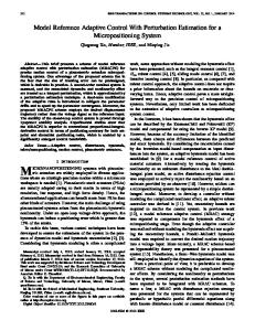
Q1 (GaAs OTPT)
INTRODUCTION
Bipolar devices such as BJTs are often preeferred for optical switching due to their ability to be directly excited, however BJTs are not always ideal for the power-switching circuits. For these applications, often power MOSFETs are considered due to relative ease of electrical contrrol and ease of fabrication. However, in contrast to the bipolar devices, where direct photo-excitation in the basee region leads to generation of electron-hole pairs, in the ppower MOSFETs, charge separation in the gate-oxide reggion (needed for channel conduction) via direct photogeneration (using charge-neutral photons) raises feasibilityy issue. Power MOSFETs typically require the aid of bipolaar devices such as photodiodes, but such a monolithic inteegration presents complications in the fabrication steps eespecially if the materials for the photodiode and the poower device are different [1]. Hybrid bonding of separrately fabricated photodiodes and power MOSFETs has shown some success in low-power devices [2]. Optical control of power MOSFETs cann provide several improvements in system parameters inncluding reduced electromagnetic interference (EMI), rrobust electrical separation, and separation of power andd control stages. Control signals, by necessity, have very largge di/dt and dv/dt values, which initiate noise problems in thee power stage and can have coupling effects. Moving these signnals to fiber-optic transmission reduces EMI and cross-talk efffects. An optical link also allows the control and driver stagess of a converter to remain separate, which can be useful for high-temperature power electronics. Such applications have become increasingly important and pervasive as pow wer semiconductor
978-1-4577-1216-6/12/$26.00 ©2012 IEEE
3 Q3 (SiC MO OSFET)
Q2 (GaAs OTPT)
(a)
(b)
(c)
Fig. 1: (a) Optically-controlled hybrid SiC device structure. (b) Cut-out of the hybrid device with a SiC power MOSFE ET (Q3) and the 2 OTPTs (Q1, Q2). (c) Device package with dual optical inteerface.
Towards that end, a solution to the optical control of a power SiC MOSFET is presented in i this paper utilizing the aid of two bipolar GaAs-based optically-triggered o power transistors (OTPTs). A solution off this nature provides the benefits of both bipolar transistors and a FETs. It also provides the advantages of GaAs, which has a higher opticalabsorption coefficient than Si, and d SiC, which has wider bandgap and higher thermal condu uctivity than Si yielding power devices with superior breakd down voltage and thermal sustenance. The OTPTs are used to o dynamically control the resistance seen by the gate of the 1200-V SiC-based power MOSFET, offering full control of the latter. Internal
2530
connections of the hybrid power device are shown in Fig. 1(a) and the actual package is shown in Fig. 1(b). A low-voltage bias is applied to the collector of the OTPT bridge. Light activates OTPTs Q1 and Q2 in a complementary manner, thereby connecting the gate of the MOSFET to the low-voltage bias and ground, respectively, turning the MOSFET on and off. Further, by controlling the intensity of the optical beam applied to the OTPTs, the resistance of the MOSFET gate drive during turn-on and turnoff as well as during conduction and dark states can be dynamically controlled. This provides a unique opportunity to activate the power MOSFET as well as control its behavior dynamically with relative ease. This paper extends the preliminary work done in [6], [7] by testing a new robust high-temperature package at 500 V, at a switching frequency of 100 kHz and higher, and by testing the hybrid power device (at converter level) using a dc/dc boost converter. The rest of this paper is presented as follows. Section II outlines the packaging information of the hybrid optically-controlled power device. Section III describes the experimental results. Finally, in Section IV, relevant conclusions are drawn. II.
optical sources powered by a pair of DEI PCX-7140 [8] current drivers were used to excite the OTPTs. The optical source was biased using a dc current of 3 A and a pulse current of 5 A (with a 50% duty cycle) for both 100-kHz and 200-kHz operation. In Fig. 2(a) the top waveforms show the negative current references of the optical pulses being delivered from the current sources, and the bottom waveform is the drain-tosource voltage of the SiC MOSFET. It can be seen that, a short pulse of high-intensity light is required to turn the OTPTs on and subsequently, charge and discharge the gate capacitance of the SiC MOSFET. This optical intensity is reduced to almost half of the initial magnitude during the steady-state (conduction) period of the SiC MOSFET. This allows Q1 to recombine some of the excess charge generated by the high-intensity pulse. A similar mechanism exists for Q2, which controls turn-off dynamics of the SiC MOSFET. Thus, the overall turn-on and turn-off times1 of the hybrid power device is reduced.
PACKAGING INFORMATION
A hybrid opto-electronic package has been designed and implemented to facilitate the photonic control of a SiC (power) MOSFET. The SiC MOSFET and the OTPT dies are placed in the same package to reduce size and parasitic loses, while providing consistent optical excitation. The vertical 1200-V SiC MOSFET is electrically insulated from the substrate of the lateral OTPTs. All three devices, however, have a thermally-conductive path through the base of the package to control junction temperature. Several thermal factors need to be considered in this package design. The difference in materials and bias conditions create a disparity in the heat produced by the different dies. Due to higher conduction and switching losses, the SiC MOSFET increases the ambient temperature inside the package, which, in turn, increases the temperature of the OTPTs. For this reason, OTPTs with a higher breakdown voltage (< 150 V) are chosen to mitigate leakage induced by increased packaged temperature. Two package configurations were tested: one with an internal connection between the middle of the OTPT bridge (i.e. the emitter of Q1 and the collector of Q2) and the SiC-MOSFET gate; the other, that places an external gate resistor between the middle of the OTPT bridge and the gate of the SiC MOSFET.
(a)
III. EXPERIMENTAL RESULTS A. Dynamic Switching of the Optically-Controlled Hybrid SiC Device The SiC MOSFET was tested with a bias voltage of 500 V and at a drain-to-source current of 0.77 A, which is controlled by a load resistance of 648 ohms. Both time-domain as well as parametric results are recorded. The OTPTs were biased with 19 V, with a 4 ohm resistance in series with the collector of Q1. Switching results were then taken at 100 kHz and 200 kHz, as shown in Figs. 2(a) and 2(b), respectively. Two 2-W
(b) Fig. 2: (bottom trace) SiC MOSFET switching dynamics (i.e. drain-to-source voltage) at (a) 100 kHz and (b) 200 kHz. Top two traces represent the laser activation signals. 1
In this paper, turn-on and turn-off times refer to the fall and rise times of the SiC-MOSFET’s drain-to-source voltage.
2531
From Fig. 2(a), a turn-on time of 100 ns annd a turn-off time of 200 ns were observed. This test was also performed at 200 kHz, as shown in Fig. 2(b). However, for the 200-kHz operation, and as can be observed from Figgs. 2(a) and 2(b), the optical pulsing of Q1 and Q2 is slightly different than the 100-kHz operation even though the minimuum and maximum intensities of the optical beams remain same. For the 200-kHz test, a 150-ns turn-on and a 350-ns tuurn-off time was recorded. An increase in the turn-off time for the 200-kHz operation is due to the slower turn off oof Q1 due to the generation of additional carriers in its base region. The turnoff speed of Fig. 2(b) does not exhibit a greeat deviation from that of Fig. 2(a). The turn-on speed is not affected by the equal-intensity pulse as much as the turn-ooff speed because no charge should be flowing through Q2 aat the moment of turn-on. Negligible delay is experienced while ussing the two-level optical control at 100 kHz. However, for the same optical intensity, the turn-on and the turn-off delayss of the OTPT are observed to be 150 ns and 250 ns, respecctively. A voltage spike can be seen during the turn off of thhe SiC MOSFET which is due to a 4.7 mH inductance off the wire-wound resistors placed in series with the SiC MO SFET and the dc voltage source for the test circuit. A parametric analysis of pulsed laser inteensity was carried out for both the OTPTs (Q1 and Q2) at 1100 kHz and 200 kHz, as shown in Figs. 3(a)-3(d). This test w was conducted by varying the intensity of the optical source off one switch while the other was held at a constant output. The results show that Q1 and Q2 operate nearly independentt of each other, allowing turn-on and turn-off of the SiC MOSFET to be controlled without any coupling. This atttains importance when implementing an active gate control sscheme to reduce the stress placed on the devices [7]. A knee is found at 5 A for both Q1 and Q Q2. After 5.5 A, a small reduction in rise and fall times are observed. From Figs. 3(a) and 3(b) it can be seen that, when usiing high intensity optical pulses, a rise and a fall time of 50 and 65 ns is obtained, respectively, when using the ma ximum output of the laser current driver.
(a)
(b)
(c)
B. Boost Converter using the Optically-Coontrolled Hybrid SiC Device After testing the switching dynamics oof the opticallycontrolled hybrid power device, a dc/dc booost converter was built using the same power device. The dioode for the boost converter was chosen to be a SiC Schottky diode to mitigate reverse-recovery losses. The boost convertter was designed for 400 W with a maximum switching frequeency of 0.5 MHz. At this frequency special care needs too be taken when dealing with parasitic inductances of the prinnted-circuit-baord (PCB) traces. A copper PCB prototype waas created on the QuickCircuit PCB prototyper. The boost coonverter test setup is shown in Fig. 4. It consists of the basic dc//dc boost
(d) Fig. 3: Switching performance of hybrid pacckaged device while varying the bridge OTPTs (a) and (b) at 100 kHz and a (c) and (d) at 200 kHz, respectively.
2532
converter was constructed and testeed experimentally. Using the OTPT bridge introduces no significant delay in the MOSFET gate drive and provides a mechanism to separate the power and the control stages. The T dc/dc boost converter was tested at 0.25 MHz. However, the switching frequency can be raised to 0.5 MHz or higher due to the fast switchingtransition dynamics of the hybrid po ower device. Because the control signals are transmitted opticcally, no distortion will be introduced due to interference durin ng signal transmission at high frequency. Finally, it is also demonstrated in this paper that, the intensity of the (OTPT) optical beam can be so optimized such that one can simultaaneously achieve fast rise and fall times as well as reduce the gate-drive loss during the conduction state of the SiC MOSFE ET by reducing the optical intensity of the OTPT.
Fig. 4: Boost converter prototype showing packaged hhybrid power device.
topology with added RC snubbers. The packaged devices, inductor, and looad resistors are mounted via thermal paste on the heat sink llocated below the board. The board is 6 cm x 10.5 cm x 7 cm, iincluding the heat sink. The boost converter was tested up to an output of 250 W, feeding a 400 ohm low-inductance reesistive load. The switching frequency was set at 0.25 MHz. Test results are shown in Fig. 5. During the testing the steady-state temperature of the power device never exceeeded 30 oC.
ACKNOWLEDGEM MENT This work is supported in part by the awards of Office of Naval Research (ONR) and the Nattional Science Foundation (NSF) monitored, respectively, by Drs. Paul Maki and George Maracus and received by Prof. Sudip K. Mazumder. However, any opinions, find dings, conclusions, or recommendations expressed herein are those of the authors and do not necessarily reflect the viiews of the ONR or NSF. The authors also acknowledge the help h of Brandon Passmore at APEI Inc. V. [1] [2] [3]
[4]
[5] Fig. 5: Dc waveform shows the output of boost convverter (328 V) and the pulsed waveform shows the drain to source voltage of thhe power MOSFET.
[6]
IV. SUMMARY AND CONCLUSIIONS Dynamic switching of a high-temperrature and highfrequency hybrid optical SiC MOSFET T package was designed and tested. The low rise and fall ttimes exhibited in the switching dynamics, proved the feasibbility of a highspeed power converter. Subsequently, a 4000-W dc/dc boost
[7] [8]
2533
REFEREN NCES
K. Kioi, T. Miyajima, M. Yoshioka, T. Doi, and KM. Koba, "SOI S for optical switching", IEEE photodiode array stacked on VDMOS Electron Devices Meeting, vol. 33, pp. 4604 463, 1987. Y. Shimizu and K. Shimomura , "Curreent modulation characteristics in optically-controlled field-effect transisto or," IEEE Photonics Technology Letters, vol. 6, no. 11, pp. 1338-1340, 1994. L.D Stevanovic, K.S. Matocha, P.A. Lo osee, J.S. Glaser, J.J. Nasadoski, and S.D. Arthur, "Recent advances in silicon s carbide MOSFET power devices," IEEE Applied Power Electron nics Conference and Exposition, pp. 401-407, 2010. omparison of SiC and Si power M.G.H. Aghdam and T. Thiringer, "Co semiconductor devices to be used in 2.5 kW dc/dc converter," International Conference on n Power Electronics and Drive Systems, pp.1035-1040, 2009. J.S. Glaser, J.J. Nasadoski, P.A. Loseee, A.S. Kashyap, K.S. Matocha, J.L. Garrett, and L.D. Stevanovic, "Diirect comparison of silicon and silicon carbide power transistors in high-frequency hard-switched applications," IEEE Applied Power Electronics Conference and Exposition, pp.1049-1056, 2011. S.K. Mazumder, and T. Sarkar, "Optically-activated gate control of power semiconductor device switching dynamics," IEEE International Symposium on Power Semiconductor Devices & Integrated Circuits, pp.152-155, 2009. S.K. Mazumder, and T. Sarkar, "Optically activated gate control for power electronics," IEEE Transactions on Power Electronics, vol. 26, no. 10, pp. 2863-2886, 2011. manual.pdf www.ixyscolorado.com/pdf/pcx-7410_m