Cut Mask Optimization for Multi-Patterning Directed Self-Assembly Lithography Wachirawit Ponghiran, Seongbo Shim, and Youngsoo Shin School of Electrical Engineering, KAIST Daejeon 34141, Korea Abstract—Line-end cut process has been used to create very fine metal wires in sub-14nm technology. Cut patterns split regular line patterns into a number of wire segments with some segments being used as actual routing wires. In sub-7nm technology, cuts are smaller than optical resolution limit, and a directed self-assembly lithography with multiple patterning (MP-DSAL) is considered as a patterning solution. We address cut mask optimization problem for MP-DSAL, in which cut locations are determined in such a way that cuts are grouped into manufacturable clusters and assigned to one of masks without MP coloring conflicts; minimizing wire extensions is also pursued in the process. Only a restricted version of this problem has been addressed before while we do not assume any such restrictions. The problem is formulated as ILP first, and a fast heuristic algorithm is also proposed for application to larger circuits. Experimental results indicate that the ILP can remove all coloring conflicts, and reduce total wire extensions by 93% on average compared to those obtained by the restricted approach. Heuristic achieves a similar result with less than 1% of coloring conflicts and 91% reduction in total wire extensions.
Cut pattern Cut cluster Regular line patterns
(a)
(b) Mask 2
Mask 1
(c) Polymer A
Polymer B
Actual routing wire
(d)
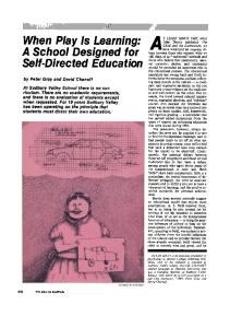
I. I NTRODUCTION As technology node scales down to sub-7nm, printing small features becomes challenging task for traditional optical lithography. MP-DSAL has recently received much attention as an alternative patterning solution due to its low manufacturing cost and high printing resolution. MP-DSAL is considered as a viable technique for printing contact and via layers [1]– [3], but its application for printing line-end cuts (or cuts for short) has also been studied [4]. In line-end cut process, regular line patterns are first created on a wafer through self-aligned double patterning (SADP) [5]; they are then split into multiple wire segments by cuts. Some segments are used as actual routing wires while the remainders become dummies and serve no function. Process to create cut patterns with MP-DSAL is as follows: cuts that are physically close are clustered (Fig. 1(a)) and contour that surrounds each cluster, called a guide pattern (GP) image, is synthesized (Fig. 1(b)). If a distance between two GP images is smaller than optical resolution limit, they are patterned on different masks (Fig. 1(c)) and actual GPs are created on a wafer by processing each mask one by one. GPs are filled with block copolymers (BCPs), which align by themselves due to forces between BCPs and GP walls during heating and annealing process (Fig. 1(d)). After one type of polymer (polymer B) is etched down to the underlying metal layer, regular line patterns are split into actual routing and dummy wires (Fig. 1(e)).
c 978-3-9815370-8-6/17/$31.00 �2017 IEEE
Ideal GP images
Dummy wire
(e)
Fig. 1. Line-end cut process with MP-DSAL: (a) regular line patterns with cut clusters, (b) ideal GP images of cut clusters, (c) multi-patterning to create GPs on a wafer, (d) GPs filled with BCP, and (e) routing- and dummy-wires created after polymer B is etched away.
Clustering nearby cuts is not arbitrary. A large and complex GP image is hard to manufacture during DSA process [6], so GP can contain only a limited number of cuts and its shape should be simple. In addition, GPs have to be assigned to one of masks without coloring conflicts. This makes cut clustering problem with mask assignment very difficult. In fact, a similar version of problem in contact and via layers has been shown to be NP-complete [1], [7]. A. Motivation and Contributions Unlike contacts and vias whose locations are fixed after layout design, cuts can be relocated to avoid coloring conflicts and forming unmanufacturable clusters. However, relocating cuts results in wire extensions as shown in Fig. 2(a). This may negatively affect circuit timing due to increased capacitance. The goal of cut mask optimization for MP-DSAL, which we address in this paper, is to determine cut locations together with cut clustering and mask assignment, in such a way that all clusters are manufacturable with smallest coloring conflicts and wire extensions are minimized. We aim to minimize coloring conflicts instead of searching for conflict-free solution
1498
Fig. 2. (a) Wire extensions after some cuts are relocated, and (b) overlap between clusters that are assigned to different masks.
because small number of conflicts can be manually fixed by designers. A restricted and simplified version of this problem has been previously addressed [4], but its solution is impractical. This is because the approach performs cut mask optimization problem for basic DSAL (without MP) independently for cuts on every three consecutive metal tracks, and implicitly assigns cut clusters on these tracks to one mask. By selecting different masks for adjacent metal track groups, coloring conflict across each group is guaranteed to be free. However, overlap may occur between clusters assigned to different masks is as shown in Fig. 2(b). In addition, assigning only one mask to clusters on each track group would limit solution space and produce result that is far from optimal (as demonstrated in Section IV through experiments). In this paper, we address the general version of cut mask optimization problem for MP-DSAL; key contributions are summarized as follows: • Cut mask optimization for MP-DSAL is formulated as ILP, which serves as a foundation for developing heuristic algorithm and is also used as a reference for comparison. • A fast heuristic algorithm is developed for application to large practical circuits. The remainder of this paper is organized as follows. Section II briefly discusses critical cut distances in MP-DSAL, and the impact of wire extensions on circuit timing. Section III presents the ILP formulation along with the heuristic algorithm. Our proposed methods are demonstrated and compared with the existing approach in Section IV. The paper is summarized in Section V. II. P RELIMINARIES A. Critical Cut Distances in MP-DSAL Suppose p denotes a center-to-center distance or pitch between two cuts; minimum pitch supported by DSAL is denoted by p− dsa ; maximum length that BCP can stretch is denoted by p+ dsa . For any two cuts to be clustered together, + their pitch must be at least p− dsa but no more than pdsa ; this range of p is marked as DSA in Fig. 3. If their pitch is larger than pmp , which is a minimum pitch supported by multipatterning, cuts can be assigned to different clusters whose GPs are patterned on different masks. This range of p is denoted as MP in Fig. 3. Hence, if a pitch between two cuts
DSA
(b)
Mask1
pmp
p+dsa
p
Mask2
p
p p
p-dsa
plitho
Fig. 3. Cut clustering and mask assignment for various cut pitches.
300 Conflict # Paths
(a)
Mask 2
MP
Mask 1
Relocated cut
Original cut
Single mask
DSA/MP
Wire extension
200 Conflict+Extension 100 Before cut optimization
0
20
Slack (ps)
40
60
(a)
200 # Paths
Dummy wire
Conflict + Extension Conflict
100
0
20
40 60 Slack difference (ps)
80
(b)
Fig. 4. (a) Slack histograms of test circuit before and after cut mask optimizations, and (b) slack changes of critical paths after cut mask optimizations.
lies in pmp ≤ p ≤ p+ dsa (marked as DSA/MP), they can be either assigned to the same cluster or assigned to different clusters whose GPs are patterned on different masks. Lastly, if a pitch between two cuts is larger than plitho , which is a minimum pitch supported by traditional optical lithography, cuts can be freely assigned to any different clusters. This range of p is marked as Single mask in Fig. 3. + The value of p− dsa and pdsa are determined by the length of BCP [8] that is employed. The value of pmp and plitho are determined from the BCP length as well as optical resolution limit, which in turn is affected by lithography settings such as wavelength of light source, NA, and illumination shape. B. Wire Extension: Impact on Timing Wire extension has been considered as a popular cost function in many existing studies of cut mask optimization [4], [9]–[11]. Nevertheless, its impact on circuit timing has never been discussed in quantitative fashion, which we try in this section using 28nm commercial library.
2017 Design, Automation and Test in Europe (DATE)
1499
Cut layout
TABLE I N OTATIONS OF THE ILP FORMULATION
GP
Fig. 5. GPs that are assumed to be manufacturable in the paper.
We obtain two optimal solutions of cut mask optimization problem using ILP (explained in Section III). The first solution (denoted by Conflitct+Extension in Fig. 4) has least number of coloring conflicts and total wire extensions. The second solution (denoted by Conflict) has the minimum number of color conflicts but wire extensions are just limited below a certain value. Slack histograms of test circuit (spi) before and after cut mask optimization are shown in Fig. 4(a). There are many paths with slack reductions after the optimizations. To justify the impact of wire extensions, we measure slack change of critical paths that originally have slack less than 50ps. As shown in Fig. 4(b), slack of critical paths in Conflict+Extension reduces by 15ps on average (and up to 72ps). Slack of critical paths in Conflict, on the other hand, reduces by 42ps on average (and up to 97ps). This large difference in slack between two optimal solutions may lead to significant timing degradation, and is also observed in other test circuits. Thus, it is reasonable to consider the total wire extensions as a cost function in cut mask optimization problem.
gi ci (xi , yi ) x �i Gik Mik Cij Oij Sij Mij pmin (i, j) h− dsa (i, j) h+ dsa (i, j) hmp (i, j) hlitho (i, j) mik Mijk W
i-th gap i-th cut Original location of cut Horizontal location of cut after optimization 1 if ci is assigned to k-th manufacturable cluster 1 if the cluster of ci is assigned to k-th mask 1 if the cluster of ci and cj have a coloring conflict; 0 otherwise 1 if (� xi , yi ) equals to (� xj , yj ); 0 otherwise 1 if ci and cj are on the same cluster; 0 otherwise 1 if the cluster of ci and cj are on the same mask; 0 otherwise Minimum pitch between ci and cj Minimum horizontal pitch between ci and cj to be on the same cluster Maximum horizontal pitch between ci and cj to be on the same cluster Minimum horizontal pitch between ci and cj to be on different clusters patterned on different masks Minimum horizontal pitch between ci and cj to be on different clusters patterned on the same mask k-th bit of mask index of cluster that ci belongs 1 if k-th bit of mask index of cluster that ci and cj belong are identical; 0 otherwise Large constant
i-th gap (gi) c2i
III. MP-DSAL CUT M ASK O PTIMIZATION Cut mask optimization for MP-DSAL determines the location of all cuts while each cut is assigned to a cluster (for DSAL) which is then assigned to a mask (for MP). It guarantees that (1) circuit connectivity remains the same, (2) total wire extensions are minimized, and (3) MP coloring conflicts are kept at a minimum. In this section, we first present ILP formulation for this problem, and move on to propose a heuristic algorithm. Note that only clusters corresponding to GPs with zero defect probability (i.e. GPs with linearly aligned cuts as illustrated in Fig. 5) are assumed.
x2i
x2i+1
We define a gap (gi ) as a space between adjacent actual routing wires on the same metal track as shown in Fig. 6(a). gi is then associated with two cuts, namely left cut (denoted c2i ) at position (x2i , y2i ) and right cut (denoted c2i+1 ) at position (x2i+1 , y2i+1 ). Without loss of generality, we assume that wires are routed on a horizontal direction. After a cut mask optimization, horizontal location of left and right cut are �2i+1 respectively while vertical location changed to x �2i and x of cuts remains the same. This leads to amount of wire �2i+1 on the right extension x �2i − x2i on the left and x2i+1 − x as illustrated in Fig. 6(b). The rest of notations used in ILP are summarized in Table I.
Wire extension
x2i
(a)
x2i+1 (b)
Fig. 6. A gap and its corresponding cuts on the left and right (a) before and (b) after the cuts are relocated.
The cut optimization problem for MP-DSAL is to determine the value of x �i , Gik , and Mik with objective to minimize total wire extensions and coloring conflicts. Minimize ��
�� � � x �2i − x2i + x2i+1 − x �2i+1 + W Cij
i
A. ILP Formulation
1500
Actual routing wire c2i+1
(1)
i,j
subject to: �
Gik = 1,
∀ci
(2)
x2i ≤ x �2i ≤ x �2i+1 ≤ x2i+1 ,
∀gi
(3)
∀ci and cj (i �= j)
(4)
k
Oij ≤ Sij ≤ Mij ,
�i ≤ x �j and pmin (i, j) ≤ p+ for all ci and cj such that x dsa , � x �j − x �i ≥ h− (5) dsa (i, j) − W (1 − Sij ) + Oij ], � + �i ≤ hdsa (i, j) + W (1 − Sij ) + Oij ], (6) x �j − x
2017 Design, Automation and Test in Europe (DATE)
for all ci and cj such that x �i ≤ x �j and pmin (i, j) ≤ pmp , � �i ≥ hmp (i, j) − W Sij + Mij ], (7) x �j − x
g1 plitho g2
g3
�i ≤ x �j and pmin (i, j) ≤ plitho , for all ci and cj such that x � � x �j − x �i ≥ hlitho (i, j) − W Sij + (1 − Mij ) + Cij , (8) for all ci and cj such that i �= j, Mijk ≥ 1 − mik − mjk , Mijk ≤ 1 − mik + mjk , Mijk ≤ 1 + mik − mjk ,
∀k ∈ {1, 2}
Mijk ≥ mik + mjk − 1,
g5
g4
g6
Actual routing wire
(a)
Potential conflict edge
(9a)
g1
∀k ∈ {1, 2}
(9b)
g2
(2)
∀k ∈ {1, 2}
(9c)
(1)
∀k ∈ {1, 2}
(9d)
4 3
5 g3 (3) 5
g4
5 g5 (2)
(2)
4
g6 (2)
(b)
2Mij ≤ Mij1 + Mij2 , Mij ≥ Mij1 + Mij2 − 1.
(10a) (10b)
Inequality (2) restricts that each cut is assigned to only one cluster. Inequality (3) specifies feasible location of cuts so that circuit connectivity remains the same. Inequality (4) guarantees that two cuts at the same location must be on the same cluster. Cuts on the same cluster must also be on the same mask. Inequalities (5)-(6) restricts that two cuts can be clustered together if their pitch is within the range of DSA (see � − 2 2 (i, j) is obtained by (p Fig. 3). h− dsa dsa ) − (yi − yj ) , and + hdsa (i, j) is obtained similarly. For any two cuts on different clusters patterned on different masks, inequality (7) restricts that their pitch is in the range of MP (see Fig. 3). If two cuts are on different clusters patterned on the same mask, inequality (8) ensures that their pitch is in the range of Single Mask (see Fig. 3). Otherwise, their clusters has a coloring conflict. Note that hmp (i, j) and hlitho (i, j) are obtained in similar manner to h− dsa (i, j). Assuming that upto four masks can be used, we represent the mask of each cluster with two-bit number mi1 mi2 in the ILP formulation. In case of double- and triple-patterning, additional constraints mi1 = 0 and mi1 + mi2 ≤ 1 should be added, respectively. A set of inequalities (9a)-(9d) is equivalent to XNOR operation (e.g. Mij1 = mi1 XNOR mj1 ), which sets Mijk to 1 if the k-th bit of mask index of cluster that ci and cj belong are identical. Inequality (10a)-(10b) correspond to AND operations (i.e. Mij = Mij1 AND Mij2 ), which determines Mij . B. Heuristic Algorithm We propose a fast heuristic algorithm which uses divide and conquer strategy to solve the cut mask optimization for large circuits. A potential conflict graph is initially constructed to represent all possible coloring conflicts during cut mask optimization. By ignoring some edges, the potential conflict graph is partitioned into many small acyclic ones. Each acyclic sub-graph is optimized independently, and the solutions of all the acyclic sub-graphs are then combined. There may still remain some coloring conflicts due to ignored edges during a potential graph partition; these conflicts are resolved through a local adjustment.
Fig. 7. (a) Example metal layout, and (b) its potential conflict graph.
Potential conflict graph construction: For a given layout, we represent each gap with a vertex as shown in Fig. 7. Potential coloring conflicts between gaps are identified based on a feasible moving region of cuts on those gaps. If gaps are closer than plitho (see g1 and g4 in Fig. 7(a)), coloring conflict may exist between their cuts during optimization. We draw an edge to represent each potential coloring conflict as shown in Fig. 7(b). Degree of each vertex (see the numbers in brackets) indicates how many potential coloring conflicts its corresponding gap has. To minimize potential coloring conflict of ignored edges during a graph partition, we try to group large-degree vertex and its neighbors together in the same acyclic subgraph. To do so, we assign each edge with a weight equal to sum of the degree of the vertices incident to it (see the numbers in red). Then, partitioning is done by ignoring all edges, and consecutively including each of them in a decreasing weight order. We exclude an edge if connecting it causes a cycle, or causes a number of the vertices in a acyclic sub-graph to exceed a certain value. The size of acyclic sub-graphs are kept small in order to partition cut mask optimization of the whole layout into many small problems. When limiting a number of the vertices in acyclic sub-graphs to 4, we partition the potential conflict graph in Fig. 7(b) into 2 sub-graphs (see solid edges). Solving acyclic sub-graph to an optimal: We convert each acyclic sub-graph into a tree by randomly picking one vertex to be a root. For instance, given the left sub-graph in Fig. 7(b), tree in Fig. 8(a) is formed by assigning g1 to be a root. Note that each tree node represents an individual gap on a layout. We then construct another graph, called configuration graph, in which each vertex (vi ) represents a feasible configuration (location, clustering, and mask) of the cuts on each gap. Some examples of vi corresponding to gap g1 and g3 are shown in Fig. 8(b). There exists an edge connecting between vi and vj if vi and vj represent configurations of the cuts on two connected gaps of a tree, and together form a valid configuration. For example, v1 is connected to v4 because v1
2017 Design, Automation and Test in Europe (DATE)
1501
Tree
(2)
Configuration graph g3
(3) (2) (0) v1 v2 v3 ...
g1
g1
g3
1
v6 0
v7 (7)
v4
0
(3) v5
(2) v6
g5 ...
g6
g5
v7
v8 (3)
v9
1
0
v9 ... (9)
v8 (3)
0
1
g6 v10 (1)
0
v11 (4)
1
(a) v12 ... (3)
1
0
Ignored edge 1
0
v11 v12 g6 v10 (1) (4) (3)
1
1
0
g5
0
(2)
g3
g3
g6
v5
0
Root
g5
v4
(b)
Fig. 9. (a) An ignored edge, and (b) configuration graph for a local adjustment.
(a) A feasible configuration of cuts Cut v1
v2
v3
,
,
g1
Coloring conflict
,
g3
,
v4
v5
v6
(b)
Fig. 8. (a) A tree and its configuration graph, and (b) example vertices corresponding to gap g1 and g3 in the tree.
represents a configuration of the cuts on gap g1 , v4 represents a configuration of the cuts on gap g3 , and gap g1 and g3 are connected on the tree. v1 and v4 also have a matching cluster on the left. However, v1 is not connected to v5 because their left clusters are different. Each vi is associated with a weight equal to amount of wire extensions (see number in brackets). If any vi and vj are connected but have a coloring conflict, their indicent edge has a weight 1 (see v1 and v4 in Fig. 8(b)). Otherwise, the edge has a weight 0 (see v2 and v5 ). Solution of acyclic sub-graph is obtained by finding a set of connected vertices {v1 , v2 , ..., vk } where each vk represents a configuration of the cuts on individual gaps of a tree. Example solution is colored with red in Fig. 8(a). The set of connected vertices with a minimum cost defined in (1) is thus the optimum solution of acyclic sub-graph. It can be obtained by transversing a tree in post-order (g5 → g6 → g3 → g1 ) and computing minimum cost (M C) at its corresponding vertices as follows. � � � min W · w(eij ) + M C(vj ) , (11) M C(vi ) = w(vi ) + c∈Ci
j
where w(vi ) is the weight of vertex vi , Ci is child node of the gap corresponding to vertex vi , j represents all configurations of cuts on the gap c, and w(eij ) is the weight of an edge between vi and vj . For illustration, the minimum cost of vertex v6 in Fig. 8(a) is computed as 2+3+1 or 6. 2 is a weight of vertex v6 itself. 3 is the minimum additional cost among configurations of cuts on gap g5 , i.e. 0+3 (v8 ) and W +5 (v9 ). 1 is the minimum additional cost among configurations of cuts on gap g6 , i.e. 0+1 (v10 ), 0+4 (v11 ), and W +3 (v12 ).
1502
Once the minimum cost of all vertices corresponding to the root gap is computed, one vertex with the smallest cost is selected. Descending vertices associated with this cost are also subsequently selected in a top-down manner, and form an optimal solution of acyclic graph. Local adjustment: After optimizing all cuts in the previous step, we check edges that are ignored during graph partitioning for any coloring conflict. If coloring conflicts exist, we try to resolve them using a local adjustment. Local adjustment is done by finding an alternative configuration of cuts on the conflicted gaps while assuming that configuration of other cuts are the same. Suppose that {v6 , v8 , v10 } is selected as a solution in the previous step. When we consider an ignored edge g5 −g6 shown in Fig. 9(a), a coloring conflict exists. New configuration with the smallest sum of edge and vertex weights is then chosen instead. That is {v6 , v8 , v11 } with total weight of 9 (see red lines in Fig. 9(b)). IV. E XPERIMENTS We implemented our algorithm with C++, and used GUROBI [12] as an ILP solver. Test circuits was taken from Open Cores [13] and ITC99 benchmark [14], and synthesized using 28-nm industrial library. M2 layout that we used is appropriately shrunk to follow sub-7nm design rule which we assume in this paper. Metal track pitch is 35nm, and corresponding cut size is assumed to be 18nm by 18nm. The number of cuts on test circuits ranges from 5k (b12) to 360k (des3 perf) as shown in Table II. Double patterning with ArF immersion lithography (1.35 NA) is assumed. Critical cut distances in MP-DSAL are assumed as follows: p− dsa = 30nm, = 45nm, p = 39nm, and p = 87nm. p+ mp litho dsa An approach proposed in [4] is also implemented for comparison. When it is applied, many conflicts (coloring conflicts + overlap) remain because overlaps between clusters assigned to different masks are ignored. Our approaches, on the other hand, guarantee to have no overlap between clusters. ILP completed the cut mask optimization for 5 small circuits (see column 5-7). Results show that ILP can remove all coloring conflicts, and reduce total wire extensions by 93% on average compared to the approach [4] being applied. Our heuristic algorithm achieves a similar result with less than 1% coloring conflict and 91% reduction in total wire extensions (see column 8-10).
2017 Design, Automation and Test in Europe (DATE)
TABLE II C OMPARISON OF THREE CUT MASK OPTIMIZATION APPROACHES
Circuits
Approach in [4] # Conflicts ΔWL (mm) 2,122 0.5 4,340 1.2 8,425 1.7 10,673 2.5 20,925 5.7 45,044 7.6 51,977 15.9 109,519 44.9 170,937 51.3 47,107 14.6
# Cuts
b12 4,776 spi 10,658 des3 area 16,164 b14 23,220 b21 46,502 aes core 79,132 b18 121,202 ethernet 280,379 des3 perf 360,624 Average
# Conflicts 0 0 0 0 0 0
100
Runtime (m) 14 27 105 134 522 161
# Conflicts 2 3 7 12 17 50 40 108 179 46
Heuristic ΔWL (%) 11% 9% 12% 10% 8% 13% 8% 8% 8% 9%
Runtime (m) 1 1 1 2 3 5 8 21 24 8
with less than 1% coloring conflict and 91% reduction in total wire extensions comparing to the existing approach. 65.9%
0% # Conflicts ILP
TP
DP
DP
DP
TP
50.1%
50
0
ILP ΔWL (%) 4% 7% 9% 8% 7% 7%
ACKNOWLEDGMENT This work was supported by the National Research Foundation of Korea (NRF) grant funded by the Korea government (MSIP) (No. 2015R1A2A2A01008037).
0% WL
# Conflicts WL Heuristic
Fig. 10. Average number of coloring conflicts and total wire extensions when cut optimization is performed for triple patterning (TP) and double patterning (DP) using ILP and heuristic algorithm.
We assumed two masks (double patterning or DP) in Table II. With three masks (triple patterning or TP), wider solution space can be explored. It allows coloring conflicts to be resolved more easily and yields less amount of wire extensions. ILP and heuristic algorithm for TP are applied to all test circuits in Table II. Average number of coloring conflicts and total wire extensions are compared in Fig. 10; the results of cut mask optimization for TP are normalized to those for DP. In TP, no coloring conflict remains after ILP and heuristic are applied. Total wire extensions are reduced by 50% with ILP. Heuristic achieves similar result with 35% reduction in total wire extensions. V. C ONCLUSION We have addressed a cut mask optimization problem for MP-DSAL. It has been formulated as ILP, and fast heuristic algorithm has also been proposed. The heuristic employs divide and conquer strategy. Potential conflict graph is constructed from a given layout and divided into many sub-graphs; each sub-graph is solved optimally. Solution of all sub-graphs are combined together, and local adjustment is performed to remove any remaining coloring conflicts due to ignored edges during graph partition. Our methods have been demonstrated in sub-7nm technology. Experimental results have indicated that our heuristic algorithm achieves a similar result to ILP
R EFERENCES [1] Y. Badr, A. Torres, and P. Gupta, “Mask assignment and synthesis of DSA-MP hybrid lithography for sub-7nm contacts/vias,” in Proc. Design Automation Conf., Jun. 2015, pp. 70:1–70:6. [2] J. Ou, B. Yu, and D. Z. Pan, “Concurrent guiding template assignment and redundant via insertion for DSA-MP hybrid lithography,” in Proc. Int. Symp. on Physical Design, Apr. 2016, pp. 39–46. [3] S. Shim, W. Chung, and Y. Shin, “Redundant via insertion for multiplepatterning directed-self-assembly lithography,” in Proc. Design Automation Conf., Jun. 2016, pp. 41:1–41:6. [4] Z. W. Lin and Y. W. Chang, “Double-patterning aware DSA template guided cut redistribution for advanced 1-D gridded designs,” in Proc. Int. Symp. on Physical Design, Apr. 2016, pp. 47–54. [5] H. Zhang, Y. Du, M. D. F. Wong, and K. Y. Chao, “Mask cost reduction with circuit performance consideration for self-aligned double patterning,” in Proc. Asia South Pacific Design Automation Conf., Jan. 2011, pp. 787–792. [6] S. Shim, W. Chung, and Y. Shin, “Defect probability of directed selfassembly lithography: fast identification and post-placement optimization,” in Proc. Int. Conf. on Computer Aided Design, Nov. 2015, pp. 404–409. [7] Z. Xiao, C. Lin, and M. D. Wong, “Contact layer decomposition to enable DSA with multi-patterning technique for standard cell based layout,” in Proc. Asia South Pacific Design Automation Conf., Jan. 2016, pp. 1–8. [8] H. Yi, X. Bao, R. Tiberio, and P. Wong, “Design strategy of small topographical guiding templates for sub-15nm integrated circuits contact hole patterns using block copolymer directed self assembly,” in Proc. SPIE Advanced Lithography, Mar. 2013, pp. 1–9. [9] Z. Xiao, Y. Du, M. D. F. Wong, and H. Zhang, “DSA template mask determination and cut redistribution for advanced 1D gridded design,” in Proc. SPIE Advanced Lithography, Mar. 2013, pp. 1–8. [10] J. Ou, B. Yu, J. R. Gao, D. Z. Pan, M. Preil, and A. Latypov, “Directed self-assembly based cut mask optimization for unidirectional design,” in Proc. Great Lakes Symp. on VLSI, May 2015, pp. 83–86. [11] Z. W. Lin and Y. W. Chang, “Cut redistribution with directed selfassembly templates for advanced 1-D gridded layouts,” in Proc. Asia South Pacific Design Automation Conf., Jan. 2016, pp. 89–94. [12] Gurobi Optimization, Inc., “Gurobi optimizer reference manual,” 2015. [Online]. Available: http://www.gurobi.com/. [13] “Opencores,” http://www.opencores.org/. [14] “ITC99,” http://www.cerc.utexas.edu/itc99-benchmarks/.
2017 Design, Automation and Test in Europe (DATE)
1503