Journal of Luminescence 94–95 (2001) 35–38
Design and modeling of waveguide-coupled microring resonator A. Belarouci*, K.B. Hill, Y. Liu, Y. Xiong, T. Chang, A.E. Craig The Spectrum Laboratory, Montana State University, PO Box 173510, Bozeman, MT 59717-3510, USA
Abstract The design and the simulation of high-Q microcavity ring resonators coupled to submicron-width waveguides are investigated. Nanofabrication results and optical properties of SiO2–TiO2 planar waveguides are presented. Key optical design parameters are characterized using Finite-Difference Time-Domain (FDTD) solutions of the full-wave Maxwell’s equations. r 2001 Elsevier Science B.V. All rights reserved. Keywords: Microring; Sol–gel; FDTD
1. Introduction Optical ring resonators are useful components for wavelength filtering, routing, switching and multiplexing/demultiplexing applications [1]. Nanofabrication makes it possible to realize optical microcavity rings that can serve as micrometer-sized switches or multiplexers-demultiplexers. Microcavity resonators may be useful in applications requiring a wide free-spectral range, such as tunable filter covering the 30-nm erbium bandwidth. TiO2–SiO2 sol–gel thin films have been used to demonstrate the design and the fabrication of ring microcavities. The use of an oxide host is motivated by the fact that it can be easily doped with rare earths. Optical quality dielectric films are basic requirements for integrated optical devices. TiO2 and SiO2 are commonly used materials in optical thin films. The large range of intermediate *Corresponding author. Fax: +1-406-994-6767. E-mail address:
[email protected] (A. Belarouci).
index values that can be obtained make them desirable in step index coatings. Interest in the use of sol–gel method to produce SiO2–TiO2 planar waveguides is due to good homogeneity, control of the composition, low process temperature, and low equipment cost.
2. Sample fabrication 2.1. Sol–gel film processing A multilayer sol–gel process has been developed in order to make SiO2–TiO2 planar waveguides on glass substrate. The process we developed to prepare the sol is similar to that reported by Dale et al. [2]. A silica-titania solution was prepared using the following procedure. TEOS was mixed with isopropanol, water and several drops of HCl to reach a pH of 2 (TEOS : isopropanol : water=1 : 4 : 4). In a separate beaker, titanium butoxide was mixed with acetylacetone (AcAc). Titanium butoxide/AcAc=0.5 was allowed to
0022-2313/01/$ - see front matter r 2001 Elsevier Science B.V. All rights reserved. PII: S 0 0 2 2 - 2 3 1 3 ( 0 1 ) 0 0 2 7 2 - 1
36
A. Belarouci et al. / Journal of Luminescence 94–95 (2001) 35–38
react for 30 min, after which the solutions were mixed together, then diluted with an equal volume solution with isopropanol. Films with a 1 : 1 molar composition of Ti/Si were deposited on glass substrates by dip-coating. Films were coated with different speeds and heat treated at different temperatures and annealing times. It is necessary to densify each gel film before the next one is deposited. The densification process is also very important in order to eliminate the pore structure resulting from the drying stage, which causes scattering losses. The optical losses of active integrated optical devices must be as low as possible. Losses are mainly due to extrinsic bulk and surface scattering. Surface scattering is directly related to the surface roughness, whereas bulk scattering is due to refractive index inhomogeneities (phase separation, crystallization or pores) and also to dust particles that can be incorporated during the fabrication process. 2.2. Device fabrication The key microcavity resonator design parameters are the coupling efficiency and the waveguide propagation loss (which is mainly due to sidewall roughness). Strong waveguide confinement dictates that the resonator-to-waveguide gap has to be very small for adequate evanescent coupling. Based on current nanofabrication technology, a realistic gap width should be B100 nm. The scanning electron microscope (SEM) image of a 10-mm-diameter ring resonator pattern is shown in Fig. 1. The adjacent waveguides are 1 mm wide. The fabricated gap width is 0.5 mm. The pattern was created in a poly(methylmethacrylate) resist layer by SEM lithography (JEOL 6100). The exposure conditions were a 15 pA probe current, a 30 kV accelerating voltage and a 10 mm working distance.
Fig. 1. SEM image of a 10-mm-diameter ring.
dependencies of the refractive index and the thickness of the films on bake time and dipping speed are plotted in Fig. 2. The thickness gradually decreases with heating time, for a given temperature, whereas the refractive index, measured at l ¼ 632:8 nm, shows a simultaneous increase. An index value of B1.57 was obtained for films treated at 1501C. An average film thickness of B1600 nm was found (2 layers), indicating a film deposition at B800 nm per layer. The attenuation was measured using a method based on the detection of the scattered light from the waveguide. Measurements of the guiding losses were performed on a propagation length of 4 cm and were found to be around 4 dB/cm. The main contribution to the propagation losses is due to dust particles introduced into the film during the multiple dip-coating processes performed in an open environment. The only way to strongly reduce the losses is to fabricate the films in a clean room.
3. Results and discussion
3.2. FDTD microcavity simulations
3.1. Physical properties
The full-wave finite-difference time-domain method of solving Maxwell’s equations has been applied [4] to the analysis of high-index-contrast waveguide-coupled microcavity rings. This
The thickness and refractive index have been measured using an ‘‘m-line’’ technique [3]. The
1.578
1900
1.576
1800
1.574
1700
1.572
1600
1.570
37
thickness (nm)
index of refraction
A. Belarouci et al. / Journal of Luminescence 94–95 (2001) 35–38
1500 1.568 1400 1.566 0
50
100
150
200
250
baking time (min) Fig. 2. Refractive index and thickness vs. bake time. The samples were baked at 1501C.
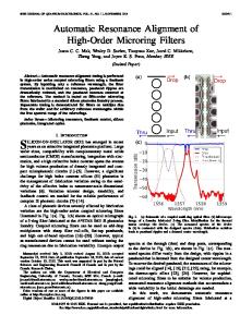
Fig. 4. Transmission response of a 10 mm-radius ring cavity.
technique has been used extensively to design complicated RF and microwave devices with dimensions comparable to the radiation wavelength. The electric field propagation off- and onresonance is depicted in Fig. 3 (ring radius=10 mm; index=1.6; waveguide width=1 mm; gap=0.1 mm). At resonance, the incident signal can be completely transferred from one bus to the other via the ring. At off-resonance, the input signal bypasses the ring. The optical bandwidth of the power transfer is mainly determined by the device size and the interaction strength between the ring and the bus. The transmission response of the cavity is reported in Fig. 4. A free spectral range of 3THz, a finesse of 15, a quality factor of 780 can be extracted from the plot. A subsequent increase of the finesse and the quality factor is expected if we increase the computation time.
4. Conclusion
Fig. 3. Electric field propagation inside the ring. (a) Offresonance at 193THz; (b) on resonance at 195.4THz.
The design and modeling of a waveguide sidecoupled to a microring has been investigated. The fabrication and characterization of planar sol–gel waveguide has been reported. Nanolithography techniques have been used to pattern the bus and the microring. Using the FDTD method, we have optimized and characterized these devices. We can achieve an
38
A. Belarouci et al. / Journal of Luminescence 94–95 (2001) 35–38
FSR as wide as 3 THz using a diameter of 10 mm. FDTD modeling has been found to be an important element in the design process of this emerging nanoscale device technology. Etching and characterization will be processed soon. We expect microcavity ring resonators to have wide application in optical communications and signal processing.
Acknowledgements This research is supported by the Department of Defense.
References [1] K. Oda, et al., IEEE PTL 7 (1995) 1447. [2] G.W. Dale, et al., Mat. Res. Soc. Symp. Proc. 180 (1990) 371. [3] R. Ulrich, R. Torge, Appl. Opt. 12 (12) (1973) 2901. [4] A. Taflove, Computational Electrodynamics: the finite– difference-time-domain method, Artech House, Norwood, MA, 1995.