ISSCC 2012 / SESSION 23 / ADVANCES IN HETEROGENEOUS INTEGRATION / 23.1 23.1
A 2.5D Integrated Voltage Regulator Using CoupledMagnetic-Core Inductors on Silicon Interposer Delivering 10.8A/mm2
Noah Sturcken1, Eugene O’Sullivan2, Naigang Wang2, Philipp Herget3, Bucknell Webb2, Lubomyr Romankiw2, Michele Petracca1, Ryan Davies1, Robert Fontana3, Gary Decad3, Ioannis Kymissis1, Angel Peterchev4, Luca Carloni1, William Gallagher2, Kenneth Shepard1 1 3
Columbia University, New York, NY; 2IBM T. J. Watson, Yorktown Heights, NY, IBM Research, Almaden, CA; 4Duke University, Durham, NC
Energy consumption is a dominant constraint on the performance of modern microprocessors and systems-on-chip. Dynamic voltage and frequency scaling (DVFS) is a promising technique for performing “on-the-fly” energy-performance optimization in the presence of workload variability. Effective implementation of DVFS requires voltage regulators that can provide many independent power supplies and can transition power supply levels on nanosecond timescales, which is not possible with modern board-level voltage regulator modules (VRMs) [1]. Switched-inductor integrated voltage regulators (IVRs) can enable effective implementation of DVFS, eliminating the need for separate VRMs and reducing power distribution network (PDN) impedance requirements by performing dc-dc conversion close to the load while supporting high peak current densities [2-3]. The primary obstacle facing development of IVRs is integration of suitable power inductors. This work presents an early prototype switched-inductor IVR using 2.5D chip stacking for inductor integration. Figure 23.1.1 shows the complete 2.5D chip stack. A prototype IC, fabricated in IBM’s 45nm SOI process, contains buck converter circuitry, decoupling capacitance and a realistic digital load. This IC is flip-chip mounted onto an interposer that holds custom fabricated coupled power inductors for the buck converter while breaking out signals and the 1.8V input power supply to wirebond pads on the perimeter of the interposer. Figure 23.1.2 shows a system level diagram of the IVR. The buck converter control circuitry resides on the IC and is composed of two control loops, a slow voltage-mode outer loop that provides low-frequency regulation and a fast inner loop that responds to high-frequency load transients. The control circuitry occupies 0.178mm2, while the bridge FETs occupy 0.1mm2. The controller is designed to accommodate any number of inductor phases up to eight, with variations of inductance values and coupling strengths. The digital pulse-width modulator (DPWM) receives an eight-bit voltage identifier code (VID), from which it derives up to eight pulse-width modulation (PWM) signals with programmable switching frequency, fs, and phase relationships. The resolution of the DPWM is limited to the 250ps period of a high-frequency reference clock provided by an on-chip PLL. The DPWM also generates an analog reference voltage, VREF, from a clean 1.8V for the outer feedback loop. The compensator for the outer feedback loop is a low-pass filter with programmable pole frequency, typically chosen 10 to 16 times lower (depending on inductance value) than the effective switching frequency Nfs, where N is the number of phases in operation. The outer feedback voltage, VFB,O, drives a delay line that modulates the DPWM output to create the reference PWM signal, VPWM, which subsequently drives the fast non-linear inner control block. The fast inner loop is shown in Fig. 23.1.2. Signal VPWM drives an RC filter to generate the inner reference voltage, VREF,I, while the bridge output voltage for each phase, VBRIDGE, drives another RC filter to generate the inner feedback voltage, VFB,I [3]. The pole in both RC low-pass filters is chosen to be below fs so that the steady state amplitude of VREF,I and VFB,I is around 150mV, which gives a small signal feedback gain of ~30V/V and ensures stable loop dynamics. In steady state, VFB,I will slew behind VREF,I and the resultant evaluation of the comparator causes VBRIDGE to closely track VPWM. In the event of a large load current transient, the error in the output voltage, VOUT, will couple across CFB onto VFB,I and the comparator will react immediately to reduce overshoot in VOUT. This fast non-linear response can reduce the required decoupling capacitance on the output voltage [3]. Also residing on the IC is a 64-tile network-on-chip (NoC) consisting of four parallel, heterogeneous, physical network planes with independent frequency domains. The NoC provides realistic load behavior and supports experimentation on supply noise and DVFS. In addition, an artificial load on the
400
• 2012 IEEE International Solid-State Circuits Conference
IC is capable of generating large current transients with ~2A/100ps slew. A total of 48nF of deep-trench (DT) and thick oxide MOS capacitance decouples VOUT and occupies 0.40mm2, while 21nF of DT occupying 0.52mm2 decouples the 1.8V input supply to compensate for the large PDN impedance. Two sets of four coupled power inductors, shown in Fig. 23.1.3, are fabricated on the silicon interposer such that one terminal of each inductor connects to a pair of VBRIDGE C4 receiving pads, while the opposite terminals are shorted and connected to several pads across the interposer for distribution of VOUT. The inductor topology is an elongated spiral with a Ni-Fe magnetic core encasing the copper windings on the long axis [4]. Similar topologies have shown high inductance density and quality factor at relevant frequencies [5,6]. The Ni-Fe magnetic alloy is chosen for its low hysteresis, high permeability and amenability to electroplating deposition. The Ni-Fe is deposited under a magnetic biasing field so that the hard axis of magnetization forms along the width of the core as shown in Fig. 23.1.3. Inverse coupling between adjacent inductors, driven with VBRIDGE signals that are ~180° out of phase, is utilized to avoid magnetic saturation of the core and consequently improve current density and ripple. The inductor fabrication involves successive electroplating deposition of the bottom magnetic core, copper windings, and top magnetic core. The windings are electrically isolated from the bottom magnetic core with a layer of silicon nitride, while a hard-baked resist process is used for electrical isolation from the top core. The hard-baked resist provides physical support to the top magnetic core and has a gentle taper to the sidewalls so that the top core arches over the windings without any abrupt transitions that would cause undesirable micromagnetic effects. The space between top and bottom magnetic cores is minimized at the device edge to provide a low reluctance path through the core and hence a large inductance. The inductance decreases and resistance increases with frequency due to eddy currents, skin effect and domain wall motion as shown in Fig. 23.1.4. Efficiency versus switching frequency and load current for the IVR chip stack are shown in Figs. 23.1.5 and 23.1.6, respectively. Efficiency peaks at 74% with input voltage of 1.8V, conversion ratio of 0.61, switching frequency of 75MHz and load current of 3A. The FEOL current density is 10.8A/mm2, which we define as load current divided by the FEOL area of the switches and controller, likewise the silicon interposer current density is 0.94A/mm2, which we define as load current divided by the total inductor area, 3.2mm2. At peak efficiency, inductor DC and AC losses contribute approximately 26% and 48% of the total power loss, respectively, while switching and conduction of the bridge FETs contribute 25%. The peak current density occurs at the thermal limit of the IC with a load current of 5.4A and efficiency of 64%. Further improvement of the inductor structures, in particular lamination of the magnetic material to reduce eddy-current losses, will significantly improve the efficiency.
Acknowledgments: This work was supported in part by the U.S. Department of Energy (DEEE0002892), the National Science Foundation (CCF-1018236 and EECS0903466), the DARPA LEAP Program, and the SRC Focus Center Research Program. References: [1] W. Kim, et al., “System level analysis of fast, per-core DVFS using on-chip switching regulators,” High Performance Computer Architecture, pp. 123-134, Feb. 2008. [2] G. Schrom, et al., “A 60MHz 50W Fine-Grain Package Integrated VR Powering a CPU from 3.3V,” Applied Power Electronics Conference and Exposition, Special Presentation, Feb. 2010. [3] N. Sturcken, et al., “An integrated four-phase buck converter delivering 1A/mm2 with 700ps controller,” IEEE Custom Integrated Circuits Conf., pp. 1-4, Sept. 2011. [4] N. Wang, et al., “Integrated On-chip Inductors With Electroplated Magnetic Yokes,” paper EH-01 at the 56th Magnetism and Magnetic Materials (MMM) Conference, Nov. 2011. (to appear) [5] D. Gardner, et al., “Review of On-Chip Inductor Structures With Magnetic Films,” Magnetics, IEEE Trans. Magnetics, pp. 4760-4766, Oct. 2009. [6] P.R. Morrow, et al., “Design and Fabrication of On-Chip Coupled Inductors Integrated With Magnetic Material for Voltage Regulators,” Magnetics, IEEE Trans. Magnetics, pp. 1678-1686, June 2011.
978-1-4673-0377-4/12/$31.00 ©2012 IEEE
ISSCC 2012 / February 22, 2012 / 1:30 PM
Figure 23.1.1: Diagram of 2.5D integrated voltage regulator (IVR) chip stack. IC with buck converter and load circuitry flips onto interposer with power inductors, which wirebonds to a ball grid array substrate.
Figure 23.1.2: Complete IVR system overview (top) and fast non-linear control loop (bottom).
Figure 23.1.3: Top view of four single-turn, coupled power inductors (left), cross-section of magnetic cores and windings (top right) and magnetization curves for the Ni-Fe core material (bottom right).
Figure 23.1.4: Inductance (L), coupling coefficient (K) and resistance (R) of coupled single-turn inductors.
23
Figure 23.1.5: IVR efficiency as a function of switching frequency.
Figure 23.1.6: IVR efficiency as a function of load current at 75MHz switching frequency.
DIGEST OF TECHNICAL PAPERS •
401
ISSCC 2012 PAPER CONTINUATIONS
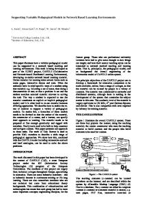
Figure 23.1.7: Photo of IC (top left), silicon interposer (bottom left) and assembled chip stack (right).
• 2012 IEEE International Solid-State Circuits Conference
978-1-4673-0377-4/12/$31.00 ©2012 IEEE