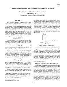
Sleep Transistor Sizing in Power Gating Designs De-Shiuan Chiou, Yu-Ting Chen, Da-Cheng Juan, and Shih-Chieh Chang Department of Computer Science, National Tsing-Hua University, Hsinchu, 30013, Taiwan Email:
[email protected] Abstract Power Gating is effective for reducing leakage power. Previously, a Distributed Sleep Transistor Network (DSTN) was proposed to reduce the sleep transistor area by connecting all the virtual ground lines together to minimize the Maximum Instantaneous Current (MIC) through sleep transistors. In this paper, we propose methodologies for determining the size of sleep transistors of the DSTN structure considering charge-balancing effect. We also introduce a new relationship among MIC, IR drops and sleep transistor networks from a temporal viewpoint and improve the sizing results. Our methods achieve significant better results than previous works. 1. Introduction Sub-threshold leakage in standby mode is an important concern for many mobile designs that rely on low threshold devices to maintain operating speed under low supply voltages [1][2]. Recently, Multi-Threshold voltage CMOS (MTCMOS) has become a popular technique for effectively reducing leakage power. Many MTCMOS structures of deploying sleep transistors have been proposed in the past. Figure 1 shows the distributed design called Distributed Sleep Transistor Network (DSTN). In the DSTN design, all the virtual ground lines (VGND) are connected together to allow the operating current from one cluster to flow through all sleep transistors [3][4]. In [3] the authors have demonstrated that due to the charge balancing effect, DSTN consistently outperforms other structures.
transistor [4]. In contrast, the IR drop across a sleep transistor in the active mode varies inversely with the size. Conventionally, this dilemma scenario can be modeled as a size minimization problem under a designer-specified IR-drop constraint. The worst-case IR drop across a sleep transistor takes place when the corresponding Maximum Instantaneous Current (MIC) flows through it. We can calculate the minimum size of a sleep transistor based on both the MIC and the IR-drop constraint. In the DSTN scenario, the charge balancing effect greatly complicates the sleep transistor-sizing problem. In [3], the size is determined directly by clusters’ MIC but ignoring the balancing effect. However, since the spirit of DSTN relies on tying all virtual ground lines together, the traditional ways of relating the independent clusters’ MIC cannot assure the quality of the final sizing. On the other hand, although the MIC through sleep transistor in the DSTN structure in Figure 1 can always be obtained by extensive simulation using tools such as Nanosim, the procedure is too slow to be practical because many time-consuming simulations are required. mA
Cluster 1
MIC(C1)
Cluster 2
MIC(C2)
Time Unit (10ps)
Low Vth Logic Cluster VDD
VGND SL Local Sleep Transistor
Figure 1. Illustration of DSTN scheme. Sleep transistor sizing is one of the most important concerns for MTCMOS designs because it immediately affects the leakage reduction and circuit performance. In the standby mode, the leakage current through a sleep transistor is proportional to the size of the sleep
Figure 2. The MIC waveforms of two clusters. In addition to the charge balancing effect, we now describe an important feature of the MIC, which greatly impact the quality of the sleep transistor sizing. Figure 2 shows the MIC distribution of two clusters of an industrial design where the MIC of each cluster occurs at different time points in a clock period. All the works [3][5][6][7] use the MIC of the clusters of the entire clock period to estimate the sleep transistor size. We observe that if a clock period is partitioned into several smaller time frames, the estimation of the MIC flowing through a sleep transistor will be more accurate. Nevertheless, optimization using many time frames leads to high computation complexity.
In this paper, we propose a novel methodology for sizing the sleep transistors in the DSTN structure and present algorithms for efficiently estimating a tight upper bound of each sleep transistor’s MIC and voltage drop considering charge balancing effect and temporal effect. The tight upper bound can be used to assure the performance penalty of inserting sleep transistors. We also derive an accurate MIC prediction across sleep transistors from cluster MICs in a temporal perspective for sleep transistor size minimization. We have observed uniform time-frame partitioning is not efficient. Hence, we propose a variable length partitioning which improves the runtime for computing an accurate IR-drop across a sleep transistor. A sizing algorithm using variable length time frames is also proposed which guarantees to converge and efficiently minimizes the total size of sleep transistors. Our sizing method outperforms all previous works in regard to the total size of sleep transistors. Both the proposed partitioning and sizing methods can be successfully applied to [3][5][6][7] to improve the sizing results. The remainder of this paper is organized as follows. In Section 2 the background knowledge is presented. In Sections 3 and 4, we propose the methodologies and algorithm for sleep transistor sizing. Section 5 gives experimental results and section 6 concludes the paper. 2. Background and Analysis In this section, we introduce the prior arts for sleep transistor sizing. Suppose IST is the current flowing through the sleep transistor, and VST is the IR drop across the sleep transistor. The width WST can be calculated as:
W ST
⎛ I ST = ⎜⎜ ⎝ V ST
⎞⎛ ⎞ L ⎟⎜ ⎟ ⎟⎜ µ C (V − V ) ⎟ TH ⎠ ⎠⎝ n ox DD
EQ(1)
The terms in the second parentheses are all constants, where L is the channel length, µn is the N-mobility, Cox is the oxide capacitance, VDD is the ideal supply voltage, and VTH is the threshold voltage of the sleep transistor. Based on EQ(1), WST is proportional to IST under a designer-specified IR-drop constraint. Hence, when the largest IST is determined, the minimum required width WST* can be described as:
⎛ MIC ( ST ) ⎞ ⎟⋅k W ST * = ⎜ ⎜ V * ⎟ ST ⎝ ⎠
EQ(2)
where VST* is the IR-drop constraint, MIC(ST) represents the MIC flowing through the sleep transistor, and k is the constant described in EQ(1). Figure 3 shows a DSTN design with three clusters. Each cluster Ci is connected to the corresponding sleep transistor STi and to other sleep transistors by virtual
ground. We define MIC(Ci) as the MIC of cluster Ci and MIC(STi) as the MIC flowing through sleep transistor STi. In general, a power gating design can be represented as a resistance network, which is a linear system as shown in Figure 4. Sleep transistors can be modeled as resistors since they operate in the linear region in the active mode [8]. The resistance value of sleep transistor STi is represented as R(STi). Logic clusters are modeled as current sources whose values depend on input patterns. Each segment of virtual ground is also modeled as a resistor. VDD
C2
C1
C3
MIC(C1)
MIC(C2)
MIC(C3)
MIC(ST1)
MIC(ST2)
VGND MIC(ST3)
ST1
ST2
ST3
Figure 3. DSTN structure. VDD
RV
RV VGND
Discharging Current
R(ST1)
R(ST2)
R(ST3)
Figure 4. Resistance network modeling. We would like to mention that MIC(Ci) calculation has been studied extensively in previous works [9][10][11][12] and is assumed given in this paper. However, because of the current discharge balance phenomenon for DSTN shown in Figure 4, the MIC(STi) cannot be calculated easily. Though MIC(STi) may be obtained through extensive post-layout simulations, it becomes impractical for a large design. The upper bound of MIC(STi) can be estimated by using the information of MIC(Ci). Taking Figure 3 and Figure 4 as an example, the relationship between MIC(Ci) and estimated upper bound MIC(STi) can be described as:
⎡ MIC ( ST1 ) ⎤ ⎢ MIC ( ST )⎥ =Ψ 2 ⎥ ⎢ ⎢⎣ MIC ( ST3 ) ⎥⎦
⎡ MIC (C1 ) ⎤ ⋅ ⎢⎢ MIC (C 2 )⎥⎥ ⎢⎣ MIC (C 3 ) ⎥⎦
⎡ψ 11 ψ 12 ψ 13 ⎤ ⎢ ⎥ and Ψ = ψ 21 ψ 22 ψ 23 ⎢ ⎥ ⎢⎣ψ 31 ψ 32 ψ 33 ⎥⎦
EQ(3)
where Ψ is a 3x3 matrix constructed from the resistance network. All the entries are positive and can be directly obtained via resistance values. After each MIC(STi) has been calculated, the required size can be directly obtained from EQ(2). 3. Sleep Transistor Sizing Methodologies In the previous section we demonstrated that a good estimation of MIC(STi) ascertains the worst case voltage drop in the virtual ground, and consequently contributes to a good sizing of sleep transistors. Hence, in this section we propose methods for deriving a tight upper bound for MIC(STi) of the sleep transistors in the DSTN structure. 3.1 Considering Charge Balancing Effect In this subsection, we describe our method which considers charge balancing effect and can efficiently estimate a tight upper bound of MIC(STi). Similar to previous works [3][5][6][7], we utilize MIC(Ci) as constraints for ICi, which is the current amount discharged from current source CSi. In this paper we assume MIC(Ci) for all clusters are known in advance. In fact, we can further obtain many different combinations of clusters’ MIC easily. For example, the maximum instantaneous current of module B1, which is composed of C1 and C2, is MIC(C1∪C2). Similarly, in this example, MIC(C1∪C2∪C3∪C4) is the MIC of all clusters, i.e. the MIC of the entire circuit. Due to the non-exclusive nature of MICs, it is always true that MIC(Ci∪Cj) ≤ MIC(Ci)+ MIC(Cj). With the clusters’ MIC information, our approach considers one sleep transistor at a time and tries to estimate MIC(STi) for the intended sleep transistor. Use ST3 in Figure 4 as an example, the problem can be modeled as a Linear Programming problem in Figure 5.
actually contains two properties that lead to very efficient computation. First, the constraint equations in this problem can be mapped into a rooted tree. Secondly, besides ψij, all the coefficients of objective function and constraint equations are positive 1s, and all variables are nonnegative. We propose an algorithm shown in Figure 6, which optimally solves the maximization problem of ISTi in linear time under the MIC constraints. We illustrate the algorithm using an example in Figure 7. Algorithm 1: IST_Upper_Bound_Estimation(j) Output: A tight upper bound of ISTj Step 1: Find i with the largest corresponding ψij. Step 2: ICi_max ← the maximized value of ICi under all the constraint equations. Step 3: Substitute ICi in all constraint equations with the value ICi_max. Step 4: Remove decision variable ICi. Step 5: If all the decision variables are determined, goto step 6. Otherwise, goto step 1. Step 6: ISTj_max ← objective function with all ICi substituted with ICi_max.
Figure 6. The exact algorithm solving the maximization problem under MIC constraints.
Decision variables: ICi, for i=1, 2, 3, 4. Objective function:
max I ST 3 = 0.21I C1 + 0.24 I C 2 + 0.35I C 3 + 0.28I C 4 Subject to: IC1 ≦ 5, IC2 ≦ 4, IC3 ≦ 8, IC4 ≦ 3,
Inputs: 1. Discharging Matrix Ψ, 2. Clusters’ MIC information MIC(Ci). Decision variables: ICi, for i=1, 2, 3, 4. Objective function:
IC1+ IC2 ≦ 7 IC3+ IC4 ≦ 10 IC1+ IC2+ IC3+ IC4 ≦ 12
Figure 7. A numerical example of MIC(STi)
max I ST 3 = I C1 ×ψ 31 + I C 2 ×ψ 32 + I C 3 ×ψ 33 + I C 4 ×ψ 34 Subject to: ICi ≦ MIC(Ci), for i=1, 2, 3, 4. IC1+IC2 ≦ MIC(C1∪C2), IC3+IC4 ≦ MIC(C3∪C4) IC1+IC2+IC3+IC4 ≦ MIC(C1∪C2∪C3∪C4)
Figure 5. A Linear Programming problem to estimate MIC(ST3). Though the LP problem shown in Figure 5 can be solved by using the traditional Simplex method, the LP problem
estimation. Consider the example in Figure 7 where our objective is to maximize IST3 given the objective function IST3 = 0.21IC1+0.24IC2+0.35IC3+0.28IC4. In step 1 of the algorithm, we first find the decision variable with the largest coefficient. In this example, IC3 has the largest coefficient 0.35. In step 2, IC3 is maximized under all the MIC constraints. In this example, the maximized IC3, IC3_max, is equal to 8. Then in steps 3 and 4, all the terms of IC3 in the constraint equations are substituted by IC3_max, 8, and the term 0.35IC3 in objective function is
removed. After that, we go back to step 1 to start the second iteration. The same process iterates in the sequence of IC3, IC4, IC2, IC1, according to the coefficient values, until all ICi_max have been determined. In this example, IC={IC1_max, IC2_max, IC3_max, IC4_max}={0, 2, 8, 2} is the final result, which leads IST3 to 3.84. 3.2 MIC Estimation Using Time-Frame Partitioning In this subsection, we describe the concept of the MIC temporal distribution, and then explain how to use that concept to estimate MIC(ST) more accurately. The concept is illustrated in Figure 8. For the simplicity of the discussion, we consider the MIC waveforms of two clusters of an industrial Advanced Encryption Standard (AES) design. In Figure 8, MIC(C1) and MIC(C2) occur at different time points. Generally, the MICs of different clusters all behave in the same. We now describe how to improve the MIC(STi) estimation using time-frame partitioning.
MIC(C2)
mA
Cluster 1 Cluster 2
MIC(C1)
Time (ps)
Figure 8. MIC(Ci) waveforms of AES. Given the waveform of MIC(Ci), we partition one clock period uniformly into several time frames and collect the MIC(Ci) of each time frame. The MIC of the ith cluster, MIC(Ci), is expanded into MIC(Ci,Tj), which means the MIC of Ci in the jth time frame. Given the MIC(Ci,Tj) information, we use EQ(3) to estimate MIC(STi,Tj): ⎡ MIC ( ST 1 ,T j ) ⎤ ⎢ ⎥ M ⎢ ⎥ =Ψ ⎢ MIC ( ST i ,T j ) ⎥ ⎣ ⎦
⎡ MIC (C 1 ,T j ) ⎤ ⎢ ⎥ M ⋅⎢ ⎥ ⎢ MIC (C i ,T j ) ⎥ ⎣ ⎦
EQ(4)
where MIC(STi,Tj) represents the MIC flowing through the ith sleep transistor in the jth time frame. Here we define IMPR_MIC(STi) as the largest value of MIC(STi,Tj) among all j. In the following, we use Figure 9 to explain that IMPR_MIC(STi) obtained from time-frame partitioning is more accurate than MIC(STi) without partitioning. With MIC(Ci) from Figure 8, we use EQ(3) to calculate the corresponding MIC(ST1) and MIC(ST2) shown as the
horizontal dotted lines in Figure 9. Then we use EQ(4) and MIC(Ci,Tj) from Figure 8 to calculate MIC(STi,Tj) for all time frames. Figure 9 shows the waveforms of MIC(STi,Tj). Furthermore, the marked two points are IMPR_MIC(ST1) and IMPR_MIC(ST2), which are 63% and 47% smaller than MIC(ST1) and MIC(ST2) respectively. mA
MIC(ST1) MIC(ST2) IMPR_MIC(ST1) MIC(ST1,Tj)
IMPR_MIC(ST2)
MIC(ST2,Tj)
Figure 9. MIC(STi,Tj) waveforms.
Time (ps)
Since the worse-case IR drop across a sleep transistor is proportional to the MIC flowing through the sleep transistor, IMPR_MIC(STi) helps to predict the IR drop more accurately than MIC(STi). 3.3 Variable Length Time-Frame Partitioning Having a large number of time frames leads to a more accurate IMPR_MIC(STi). However, it also leads to high computation complexity. In this section, we use a technique of variable length time-frame partitioning to significantly reduce the complexity with only a slight loss in the accuracy of the IMPR_MIC(STi) estimation. We first give a definition and a lemma. Definition 1: For two different time frames Ta and Tb, Ta dominates Tb if MIC(Ci,Ta)>MIC(Ci,Tb) for all i. Lemma 1: If Tb is dominated by Ta, then MIC(STi,Ta)> MIC(STi,Tb) for all i. For example, Figure 10(a) shows the MIC(Ci) distribution of a uniform ten-way partition. In Figure 10(a), time frame T3 is dominated by T6 because MIC(C1,T6) is larger than MIC(C1,T3) and MIC(C2,T6) is larger than MIC(C2,T3). From Lemma 1, we have that MIC(STi,T6) are larger than MIC(STi,T1) for all i. As a result, we can neglect T3 when calculating IMPR_MIC(STi). In this case, T1, T4, T5, T7, T8, and T10 are also dominated by T6. We can remove the dominated time frames to reduce the complexity. Now we discuss another important feature of the partitioning. Figures 10(b)(c) show two different ways of two-way partition. Figure 10(b) illustrates a uniform two-way partition while Figure 10(c) shows a variable length two-way partition. Since MIC(Ci,Tb) for all i in time frame Tb in Figure 10(b) are larger than MIC(Ci,Tc) and MIC(Ci,Td) in Figure 10(c), IMPR_MIC(STi) in Figure 10(c) will be smaller than in Figure 10(b). This
example shows that if all the MIC(Ci) are separated in different time frames, the IMPR_ MIC(STi) can be better estimated.
mA
T1 T2 T3 T4 T5 T6 T7 T8 T9 T10 Cluster 1
MIC(C1,T6)
MIC(C1,T3)
Cluster 2
MIC(Ci,Tj), we are able to evaluate MIC(STi,Tj) according to EQ(4). After that we update Slack(STi,Tj) for each sleep transistors in all time frames. In the second step, we search the worst slack and enlarge the corresponding sleep transistor according to MIC(STi,Tj). Since the size has been modified, we can update Ψ, MIC(STi,Tj), and the improved Slack(STi,Tj) in the given order. Then, we perform the sizing algorithm in step 2 iteratively until all slacks are equal to or greater than zero, which means the IR drop constraint is satisfied.
MIC(C2,T6) Algorithm: ST_Sizing(MIC(Ci,Tj), DROP_CONSTRAINT) 1:
MIC(C2,T3) (a) A ten-way partition. mA
Ta
Time Unit (10ps)
Cluster 1 Cluster 2
MIC(C2,Ta)
6: update Ψ, MIC(STi,Tj), and Slack(STi,Tj) for all i,j; 8: repeat 9: 10: 11:
MIC(C1,Ta) Time Unit (10ps)
Td
MIC(C1,Tc)
min_slack ← MAX; for i ← 1 to NUM_CLUSTER, j ← 1 to NUM_TF if (Slack(STi,Tj)<min_slack) then
12:
min_slack ← Slack(STi,Tj);
13:
i* ← i;
14: 15:
(b) An inefficient two-way partition.
Tc
R(STi) ← MAX;
5: end for 7: /* step 2: sizing */
MIC(C2,Tb)
mA
3: for i ← 1 to NUM_CLUSTER 4:
Tb
MIC(C1,Tb)
Output: A set of decision variables R(STi)
2: /* step 1: initialization */
j* ← j; end if
16:
end for
17:
R(STi*) ← DROP_CONSTRAINT∕MIC(STi*,Tj*);
18:
update Ψ, MIC(STi,Tj), and Slack(STi,Tj) for all i,j;
19: until Slack(STi,Tj)≧0 for all i,j
MIC(C2,Td)
20: return R(STi) for all i;
Figure 11. Sleep transistor-sizing algorithm.
MIC(C2,Tc) MIC(C1,Td) Time Unit (10ps)
(c) An efficient two-way partition. Figure 10. MIC(Ci,Tj) waveforms of different partitions. 4. Efficient Sleep Transistor Sizing Algorithm In this section we propose a sizing algorithm considering the properties of the current balancing effect of DSTN and temporal effect of the MIC. We first define the voltage slack, Slack(STi,Tj), as the difference between the drop constraint and the product of MIC(STi,Tj) and R(STi). The details of our sizing algorithm are presented in Figure 11. In the first step, all R(STi) are initialized with a large value. Each time after the sizes are determined, we can obtain a new discharging matrix Ψ. With Ψ and
5. Experimental Results In our experiments, we implement the sizing methods of [3] and V-TP. V-TP represents our sizing algorithm with the variable length 20-way partition. All methods are applied to both MCNC benchmark circuits and an industrial AES design for comparison. The TSMC 130nm CMOS technology process is used in our experiments. Additionally, the virtual ground resistance is set to 0.057 ohm per micron according to the process data. Table 1 shows the experimental results. Column 1 provides the name of benchmark circuits and Column 2 shows the gate counts. Columns 3 and 4 show the sleep transistor sizing results from [3] and V-TP, respectively. Take circuit t481 as an example. The sizing result is 9405 µm from [3] and 5402 µm from V-TP. The bottom row shows the average sizing results normalized to V-TP. On average, our V-TP method achieves 37.5% size reduction when compared to [3]. The results clearly
demonstrate that our method always achieves impressive size reduction on both benchmarks and the industrial design. Table 1. Sizing results comparisons. Circuit Gate Count Total Area (Width in µm) [3] V-TP C432 334 12817 7086 C499 316 10741 7229 C880 466 15050 9676 C1355 339 19352 11496 C1908 361 11859 7565 C2670 295 5420 2756 C3540 1010 29808 20282 C5315 1248 29794 19534 C7552 1687 41016 25621 dalu 2395 3468 2283 frg2 1712 3632 2255 i8 3781 13247 8141 t481 5316 9405 5402 des 6175 11804 8145 AES 40097 44378 28137 Avg. 1.60 1
Gate Clustering Technique,” Proc. of the DAC, pp. 480-485, 2002. [6] J. Kao, A. Chandrakasan, and D. Antoniadis, “Transistor
Sizing
High-Speed
Digital
Circuit
Technology
with
Multi-Threshold Voltage CMOS,” IEEE Journal of Solid-State Circuits, vol. 30, no. 8, pp. 847-854, Aug. 1995. [8] J. Kao, A. Chandrakasan, and D. Antoniadis, “Transistor
Sizing
Issues
and
Tool
for
Multi-threshold CMOS Technology,” Proc. of the DAC, pp. 409-414, 1997. [9] C. T. Hsieh, J. C. Lin, and S. C. Chang, “A Vectorless
“Parametric Yield Estimation Considering Leakage Variability,” Proc. of the DAC, pp. 442-447, 2004. [3] C. Long and L. He, “Distributed Sleep Transistor Network for Power Reduction,” IEEE Transactions on VLSI Systems, vol. 12, no. 9, pp. 937-946, Sep. 2004. [4] K. Shi, and D. Howard, “Challenges in Sleep Transistor Design and Implementation in Low-Power Designs,” Proc. of the DAC, pp. 113-116, 2006. [5] M. Anis, S. Areibi, M. Mahmoud, and M. Elmasry, Reduction
for
Shigematsu, and J. Yamata, “1-V Power Supply
[1] H. Chang and S. S. Sapatnekar, “Full-Chip Analysis of Leakage Power Under Process Variations, Including Spatial Correlations,” Proc. of the DAC, pp. 523-528, 2005. [2] R. R. Rao, A. Devgan, D. Blaauw, and D. Sylvester,
Power
Tool
[7] S. Mutoh, T. Douseki, Y. Matsuya, T. Aoki, S.
Estimation of Maximum Instantaneous Current for Sequential Circuits,” Proc. of ICCAD, pp. 537-540, 2004. [10] H. Kriplani, F. Najm, and I. N. Hajj, “Pattern Independent Maximum Current Estimation in Power and Ground Buses of CMOS VLSI Circuits: Algorithms,
Leakage
and
DAC, pp. 409-414, 1997.
References
and
Issues
Multi-threshold CMOS Technology,” Proc. of the
6. Conclusions We have presented a new algorithm for reducing the leakage of a power gating design. The main idea of our method is to consider the charge balancing effect and introduce the fine-grained MIC(Ci) within a clock period from a temporal perspective. On average our sizing algorithm can achieve 37.5% size reduction than [3].
“Dynamic
MTCMOS Circuits Using an Automated Efficient
in
Signal
Correlations,
and
their
Resolution,” IEEE Transaction on Computer-Aided Design of Integrated Circuits and Systems, vol. 14, no. 8, pp. 998-1012, Aug. 1995. [11] C. Y. Wang and K. Roy, “Maximization of power dissipation in large CMOS circuits considering spurious transitions,” IEEE Transaction on Circuits and Systems, vol. 47, no 4, pp. 483-490, Apr. 2000. [12] Synopsys Inc. PrimePower Version-X 2005, 12 – User’s Manual.