Indian Journal of Engineering & Materials Sciences Vol. 14, April 2007, pp. 163-166
Strain induced non-linear conduction in epitaxial La0.7A0.3MnO3 manganite thin films P S Vachhani, P S Solanki, J H Markna, R N Parmar, J A Bhalodia & D G Kuberkar* Department of Physics, Saurashtra University, Rajkot 360 005, India Received 19 July 2006; accepted 20 February 2007 In this paper, the current-voltage (I-V) properties of La0.7A0.3MnO3 (A = Ca, Sr, Ba) manganite thin films grown on single crystalline LAO (100) substrate using chemical solution deposition (CSD) technique have been reported. Epitaxial nature of all the films has been confirmed from XRD measurements. The I-V measurements carried out on La0.7Ba0.3MnO3 (LBMO) films show an unusual non-linear transport behaviour contrary to that observed for La0.7Ca0.3MnO3 (LCMO) and La0.7Sr0.3MnO3 (LSMO) films. This non-linearity has been explained in terms of non-uniform strain distribution resulting due to mismatch in the lattice parameters of LBMO film and substrate. The conductance data for all the films have been fitted using Simmon’s model and the possible mechanism of charge conduction in the films has been discussed. IPC Code: H01F10/00
There has been extensive research work carried out on the manganites having general formula R1-xAxMnO3 (R= rare earth trivalent cation, A= divalent cation). These systems exhibit dual novel properties such as negative colossal magnetoresistance (CMR) and the metal-insulator (M-I) transition in the vicinity of magnetic transition (paramagnetic to ferromagnetic) which have been explained in terms of correlation between spin, charge and orbital degrees of freedom1. It is well-known fact that, Zener-double exchange (ZDE) is responsible for the ferromagnetic metal to paramagnetic insulator (FMM-PMI) transition but one cannot account that this is the only reason for the FMM-PMI transition2. The Jahn-Teller (JT) distortion should be considered along with the ZDE which suggests that, the lattice distortion caused by Mn3+ ion (bond stretching in the MnO6 octahedra) also plays a crucial role in M-I transition and the suppression in resistivity3. Moreover, since last few years the efforts have been made on the fabrication of devices based on manganite thin films and multilayers, having potential applications. To understand the transport behaviour of such devices, I-V characteristics emerge as a most comprehensive tool. There are few reports on the creation of an artificial grain boundaries on the thin film structures by depositing the films on the bicrystal substrates4,5. Studies on effect of grain _________________ *For correspondence: (E-mail:
[email protected];
[email protected])
boundaries in La1-x(Sr/Ca)xMnO3 thin films grown on bi-crystal substrates suggest that, the transport properties of the film cannot be fully explained by tunnelling across grain boundary5. Gunnarsson et al.6 have demonstrated the model for spin-polarized transport through artificial grain boundary created by bi-crystal substrates which correlates the magnetoresistance value with the potential barrier at the grain boundary. Khare et al.7 have investigated the conduction through an artificial grain boundary junction made in LBMO thin film with optimal doping. In the course of present studies, all the manganite thin films were grown using simple and faster chemical solution deposition (CSD) technique which yield high quality epitaxial films of desired thickness. The advantage of CSD technique for thin film growth over the other techniques is in its requirement of low reaction and annealing temperatures and cost effectiveness. In this communication, the results of the temperature dependent I-V studies on LCMO, LSMO and LBMO manganite thin films grown by CSD method have been explained and the results obtained have been discussed in the context of possible conduction mechanism. Experimental Procedure The La0.7A0.3MnO3 (A = Ca, Sr, Ba) thin films were grown by dissolving the constituent acetates in a mixture of acetic acid and water to obtain precursor
164
INDIAN J. ENG. MATER. SCI., APRIL 2007
solution. Precursor solution was used for the deposition of films on single crystalline LAO (h 0 0) substrates using automated spin coater unit. These deposited films were then subjected to drying and calcinations at different temperatures and were finally annealed in controlled oxygen atmosphere at 1000°C for 12 h. Structure and phase purity of the films were studied using X-ray diffraction (XRD) and the atomic force microscopy (AFM) was used for obtaining the information about surface morphology of grains. The I-V measurements were performed using standard d.c. four probe method, applying the current ranging between 1 µA-1 mA at various constant temperatures. Results and Discussion Analysis of the XRD data shows that, all the films are single phasic in nature and are (0 0 l) oriented. The thickness of all the films was estimated to be ~150 nm using the AFM data. From R-T measurements, the insulator-metal transition temperatures, Tp, were found to be ~ 250, 360 and 325 K for LCMO, LSMO and LBMO films, respectively.
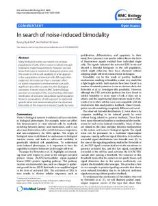
Mn4+ ion8, while the in-plane strain (either compressive or tensile) in epitaxial thin films induces larger amount of JT distortion in the structure which in turn affects the itinerant electrons and tend to localize them. In the presently studied LBMO thin film sample, the in-plane lattice constant value for LBMO is ~ 3.904 Å and for the LAO substrate it is ~3.788 Å. The calculated value of strain using δ = dsubstrate – dthin film/dsubstrate × 100 in LBMO film is -3.062% (compressive strain). This suggests that LBMO film exhibits large compressive strain as compared to the reported values of ~ -2.0% for LSMO and ~ -1.81% for LCMO films9,10. The existence of large compressive strain in LBMO film (~3%) can be attributed to the presence of island growth in the grain structure of the film, as shown in the AFM photographs [Fig. 2]. It is reported that, island growth leads to highly non-uniform distribution of strain11. The top of the islands are low strained regions while the edges are highly strained regions. This kind of non-uniformity in the strain, results into two different regions, a highly strained region acting as an insulator while low strained region acting as a metallic region. Therefore, the small
Current-voltage characteristics
I-V characteristics for all the films were measured in current-in-plane (CIP) geometry as a function of temperature. The maximum current applied to the film was 1 mA and different temperatures at which IV data was collected were 82 K, 110 K, 150 K, 200 K and 300 K. I-V measurements show similar behaviour for forward and reverse applied voltages. Fig. 1 displays the I-V data for increasing bias voltages showing that the slope of the curves is inversely proportional to the temperature. The fitting of the I-V data in the power law of the form I α Vα
… (1)
where, α is a temperature and field dependent parameter depicts that, the I-V behaviour is slightly non-ohmic for LCMO and LSMO films. The α value increases marginally from 1.005 to 1.142 for LCMO and 1.02 to 1.1 for LSMO with increasing the temperature from 82 K to RT. The observed non-linearity in I-V behaviour of LBMO film [Fig. 1c] can be understood as follows: It is reported that the hydrostatic external pressure or chemical pressure produced by larger divalent cation doping at A-site increases the hopping of eg electron from Jahn-Teller (JT) Mn3+ ion to non-JT
Fig. 1— Current-voltage (I-V) characteristics at 82, 110, 150, 200 and 300 K for (a) LCMO, (b) LSMO and (c) LBMO
VACHHANI et al.: EPITAXIAL La0.7A0.3MnO3 MANGANITE THIN FILMS
165
Fig. 2— AFM picture of LBMO thin film
insulating regions surrounded by metallic ones behave as a small thin barrier between two metallic regions. Consequently, the tunnelling through these insulating regions causes the non-linearity in the I-V characteristics. Conductance-voltage analysis
Fig. 3 shows conductance versus voltage plots for CSD grown LCMO, LSMO and LBMO films obtained at different temperatures. It can be seen from the plots that, conductance increases with applied voltages for all the temperatures which is attributed to the electron tunneling process predicted by Simmons model12 described as, G (dI/dV) = a + bVn
… (2)
where a is the zero-bias conductance at a particular temperature, b is the co-efficient which depends on potential barrier and n is the constant whose value can predict the kind of electrical transport mechanism. The values of n, for the films studied, were obtained after fitting the conductance data in Simmon’s model as given in Eq. (2). n ≥ 0.6, indicates tunneling through disordered metallic oxides13, while n = 4/3 indicates quasiparticle tunnelling via pairs of localized states14. If n > 1.4, it indicates for spin-flip scattering at the grain boundary15 and n = 2 predicts the direct tunnelling of charge carriers. In the present work, for LCMO sample, the value of n is ~1.3 at 200 K and at 300 K it becomes 1.59 which suggests that the transport through quasi-
Fig. 3— Conductance-voltage (dI/dV-V) characteristics at 82, 110, 150, 200 and 300 K for (a) LCMO, (b) LSMO and (c) LBMO
particle tunnelling via pairs of localized states dominates at the temperature around 200 K while at 300 K, the spin-flip scattering at the grain boundaries becomes prominent mechanism of conduction. For
166
INDIAN J. ENG. MATER. SCI., APRIL 2007
LSMO, the value of n is ~ 0.7 at 82 K which indicates the disordered metallic oxide type conduction behaviour whereas the variation in the n value between 1.18-1.44 obtained for 150-200 K points towards the quasiparticle tunnelling of charge carriers. At 300 K, the value of n is ~1.65 suggesting that spin-flip scattering at grain boundaries is prominent in LSMO sample. In the case of LBMO sample, the electrical transport is dominated by tunnelling through disordered oxides up to 200 K as n value varies between 0.68-0.72 which rapidly increases to 1.56 at 300 K indicating the spin-flip scattering of charge carriers.
Acknowledgement This work has been carried out under the financial support in the form of Center of Excellence (CE) project sanctioned by GUJCOST, Gandhinagar, India. References 1 2 3 4 5 6
Conclusions From the results of the I-V measurements and the fitting of the conductance data in Simmon’s model for LCMO, LSMO and LBMO manganite thin films studied, it can be concluded that, the spin-flip scattering becomes dominant at room temperature. The non-linear transport behaviour observed in epitaxial LBMO thin film can be attributed to the large in-plane compressive strain caused due to the large mismatch in the in-plane lattice parameters of the film and substrate. The mismatch causes nonuniform strain distribution in the film which results into two different strained regions and the tunnelling of carriers through the highly strained insulating region is responsible for non-linearity in the I-V characteristics.
7 8 9 10 11 12 13 14 15 16
Rao C N R & Raveau B, CMR, charge ordering and related properties of manganese oxides (World Scientific, Singapore), 1998. Tokura Y, Colossal Magneto-resistive Oxides (Gordon and Breach Science, Netherlands), 2000. Zener C, Phys Rev, 82 (1951) 403. Millis A J, Littlewood P B & Shraiman B I, Phys Rev Lett, 75 (1995) 5144. Blamire M G, Schneider C W, Hammerl G & Mannhart J, Appl Phys Lett, 82 (2003) 2670. Todd N K, Mathur N D, Evettes J E & Blamire M G, J Appl Phys, 85 (1999) 7263. Gunnarsson R, Kadigrobov A & Ivanov Z, Phys Rev B, 66 (2002) 024404. Khare Neeraj, Moharil U P, Gupta A K, Raychaudhury A K, Pai S P & Pinto R, Appl Phys Lett, 81 (2002) 325. Millis A J, Darling T & Migliori A, J Appl Phys, 83 (1998) 1588. Bibes M, Valencia S, Balcells L I, Martinez B, Fontcuberta J, Wojcik M, Nadolski S & Jedryka E, Phys Rev B, 66 (2002) 134416. Tsui F, Smoak M C, Nath T K & Eom C B, Appl Phys Lett, 76 (2000) 2421. Biswas Amlan, Rajeswari M, Srivastava R C, Li Y H, Venkatesan T, Greene R L & Millis A J, Phys Rev B, 61 (2000) 9665. Simmons J G, J Appl Phys, 34 (1963) 1793. Raychaudhury A K, Adv Phys, 44 (1995) 21. Glazman L I & Matveev A K, Sov Phys JEPT, 67 (1998) 1276; Zh Eksp Teo. Fiz, 94 (1988) 332. Guinea F, Phys Rev B, 58 (1998) 9212.