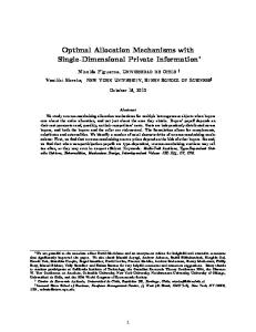
2D Self-Aligned Via Patterning Strategy with EUV Single Exposure in 3nm Technology Suhyeong Choia , Jae Uk Leeb , Victor M. Blanco Carballob , Ryoung-Han Kimb , and Youngsoo Shina a School
of Electrical Engineering, KAIST, Daejeon 34101, Korea b imec, Kapeldreef 75, B-3001 Leuven, Belgium ABSTRACT
EUV lithography (EUVL) is rising up as a solution of sub-10nm technology node via patterning. Due to better resolution of EUVL than it of immersion ArF (iArF) lithography, multiple iArF masks can be replaced by one EUV mask. However, for 24nm by 24nm metal grid, two diagonally neighboring vias yield either contour of two holes or peanut-shape contour. Because of the large variability of the via contours, the two vias are separably patterned with two different masks. We propose to insert bridge patterns (BPs) at the middle of the diagonally neighboring vias, so that single EUV exposure can draw peanut-shape contour consistently. In this study, we also assume 2D self-aligned via (2D SAV) which can align via holes in both vertical and horizontal direction for better edge placement error margin, so unique re-targeted via patterns that is called bridged via (BV) appears. We investigate impact of BV size and BP shapes on simulated contour using source mask optimization, and popular BVs are compared in terms of probability of failure which are calculated with Monte-Carlo simulation. Keyword: EUV lithography (EUVL), 2D self-aligned via (2D SAV), bridge via (BV), via bridging, via necking, source mask optimization (SMO)
1. INTRODUCTION EUV lithography (EUVL) is a promising replacer of immersion ArF (iArF) lithography for advanced technology nodes (e.g. sub-10nm).1 Thanks to short wave length of 13.5nm, EUVL can save the manufacturing cost by using single EUV mask instead of multiple masks of iArF lithography.2 However, edge placement error (EPE) still remains as a challenge because EUVL process variations such as resist stochastic and mask 3D (M3D) effect3 are critical in sub-10nm nodes. To obtain more EPE budget, 2D self-aligned via (2D SAV) which is self-aligned
Material A
Hard mask
Re-targeted via
Via
Photo resist Hard mask
Etch
Etch
Material A Mx layer
Dielectric
Mx+1
Metal
Mx
Mx+1 layer
(a)
(b)
(c)
Figure 1. (a) Top-down view of 2D SAV with original and re-targeted via patterns, (b) horizontal, and (c) vertical cross-sectional views after selective etch. Extreme Ultraviolet (EUV) Lithography VIII, edited by Eric M. Panning, Kenneth A. Goldberg, Proc. of SPIE Vol. 10143, 1014321 · © 2017 SPIE · CCC code: 0277-786X/17/$18 · doi: 10.1117/12.2257923
Proc. of SPIE Vol. 10143 1014321-1 Downloaded From: http://proceedings.spiedigitallibrary.org/ on 04/02/2017 Terms of Use: http://spiedigitallibrary.org/ss/termsofuse.aspx
Via
Re-targeted pattern
Re-targeted pattern
Mx layer
Kissing corner
Mx+1 layer
(a)
(b)
(c)
Figure 2. (a) Diagonally neighboring two vias and its lithography simulation results: (b) peanut-shape contour and (c) contour of two holes. BV Manhattanized diagonal bar BP
Diagonal bar BP
Square BV
Mx layer
BP size Re-targeted via size Mx+1 layer
(a)
(b)
(c)
Figure 3. Three BVs with different BPs: (a) square, (b) diagonal bar, and (c) Manhattanized diagonal bar.
in both Mx and Mx+1 layers has been conceptually introduced.4 As shown in Figure 1(a), material A and hard mask run alternately within both Mx and Mx+1 layers. Re-targeted via pattern is slightly larger than original via pattern in both directions, so that the via pattern is always exposed under variations of lithography (as well as etch). During etch process, material A and dielectric are eliminated while hard mask remains thanks to their etch selectivity, so that final via hole is aligned in horizontal and vertical directions as shown in Figure 1(b) and (c), respectively. However, metal grid size arrives at 24nm by 24nm, EUVL with 2D SAV also demands two masks due to limitation of current wafer inspection algorithm. In the grid, the closest vias are diagonally located in the center to center (C2C) distance of 34nm as shown in Figure 2(a). Corners of the re-targeted patterns touch each other, so called kissing corner, and either contour of two holes or peanut-shape contour are obtained under process variations (e.g. does, focus, and mask error) as illustrated in Figure 2(b) and (c).5, 6 Although both contours can be safely translated to two via holes thanks to 2D SAV integration characteristics, either of them is detected as a defect by after-develop inspection (ADI) tool. During ADI, SEM image of every die is captured and compared to reference SEM image which is ideally repaired by E-beam, and if the captured image is different from the reference one, the different patterns are flagged as defects.7 Thus, two EUV masks are needed for via patterning in 24nm by 24nm metal grid to avoid generating some thousand of defects in ADI.
Proc. of SPIE Vol. 10143 1014321-2 Downloaded From: http://proceedings.spiedigitallibrary.org/ on 04/02/2017 Terms of Use: http://spiedigitallibrary.org/ss/termsofuse.aspx
Low-k dielectric
Spacer Madrel
(a)
Metal
(b)
(c)
(d)
Photo resist Rotation
Etch
Hard mask
(h)
(g)
Material A
(f)
(e)
Figure 4. Illustrative integration flow of 2D SAV.
We propose a bridged via (BV) to keep the EUV mask count as one in the metal grid. We insert a bridge pattern (BP) at every kissing corner during re-targeting as illustrated in Figure 3(a), so that we intentionally generate only a peanut-shape contour; the contour is now consistent, so the contours pass ADI. We propose evaluation metric of BVs and demonstrate source mask optimization (SMO) for some combinations of different sizes of BPs and re-targeted vias taking EUVL-induced process variations into account. As a result, we figure out a proper BV solution which satisfies reasonable mask rules (e.g. minimum segment length, minimum feature distance, SRAF rules). We then manipulate the shapes of BP as illustrated in Figure 3(b) and (c) for further optimization of BV. While a few nm difference of BP shapes, which is smaller than EUV wave length is not noticeable for EUV source, OPC engine sets evaluation points differently and provides distinguishable OPCed masks (and corresponding contours). Frequently appearing BVs in a test layout are compared in terms of probability of failure which are calculated by Monte-Carlo simulation. The remainder of this paper is organized as follows: In the next section, one possible 2D SAV integration flow is presented. In Section III, initial BV mask synthesis and its association with current OPC tool are described. Assessment of proposed BVs is demonstrated in Section IV, and Section V summarized this paper.
2. INTEGRATION OF 2D SAV We propose an illustrative integration flow of 2D SAV as follows: The spacer is deposited around mandrel and on low-k dielectric (Figure 4(a)). The spacer is etched back, so a trench is formed in between the mandrel lines (Figure 4(b)). Mandrel is selectively etched while spacer is intact, and low-k dielectric is subsequently etched to form a trench for metalization within Mx layer (Figure 4(c)). Metal is filled in the trench, and chemical mechanical planarization (CMP) is performed to remove over grown metal; the metal is then recessed
Proc. of SPIE Vol. 10143 1014321-3 Downloaded From: http://proceedings.spiedigitallibrary.org/ on 04/02/2017 Terms of Use: http://spiedigitallibrary.org/ss/termsofuse.aspx
Outer contour
Inner contour
Critical margin
Mx layer
Bridge width
Mearsurment line
Mx+1 layer
Figure 5. Evaluation metrics of BV: bridge width and critical margin. Table 1. Corner process conditions
Focus error (nm) ±40
Dose error (%) ±5
Mask error (nm) ±0.25
Flare error (%) ±1
Image blurring (nm) 3
to be desired thickness (Figure 4(d)), so far it is very similar to metal trench formation of self-aligned double patterning (SADP) process. We now deposit dielectric material A, and planarization and recess are following similarly to metal formation (Figure 4(e)). The rest of the spacer and low-k dielectric are selectively etched in the sequence while material A is intact; hard mask is also shallowly deposited and recessed to be positioned only in between material A (Figure 4(f)). Figure 4(f) is then 90◦ rotated and Figure 4(a) is piled up on the top of it as illustrated in Figure 4(g) to integrate Mx+1 layer. processes in Figure 4(b), (c), and (f) are repeated from this step; metalization is excluded this time. At last, Figure 4(h), which is ready for via patterning, is turned out. Via and metal within Mx+1 layer are formed following procedures. Resist is spin-coated on the top and exposed with via mask which is optimized from re-targeted via patterns. Although the resist on the hard mask may also be developed due to largely re-targeted via pattern, only material A is etched, and via hole is open as illustrated in Figure 1(b); as shown in Figure 1(c), material C on dielectric of Mx layer also play a role of etch stopper. Material A, low-k dielectric, and material A should be sequentially etched to open the hole until metal within Mx layer, so if possible, it is better that material A and low-k dielectric have similar etch rates to be eliminated by once; the use of a chamber for etch reduces process variability. After the selective etch process, metal trench is defined by lithography and etch on some regions of material A. We finally fill metal into the via hole and the trench together which is called via first dual-damascene process.
3. BRIDGED VIA MASK SYNTHESIS 3.1 Evaluation Metrics For one BV which is a combination of BP and re-targeted via, multiple OPCs are processed to consider various corner process conditions as provided in Table 1, and we evaluate the BV using the simulated contours. We propose three metrics such as the bridge width, critical margin, and process variation band (PVB) width, which are measured from the contours. Bridged width is the width of a contour which is measured along measurement line as illustrated in Figure 5; the measurement line is perpendicular to via center to center connection line and crosses middle point of it. If contour of two holes are obtained from simulation instead of peanut-shape one,
Proc. of SPIE Vol. 10143 1014321-4 Downloaded From: http://proceedings.spiedigitallibrary.org/ on 04/02/2017 Terms of Use: http://spiedigitallibrary.org/ss/termsofuse.aspx
2 18
20
22
24
Max. PVB width [nm]
4
Min. critical margin [nm]
Min. bidge width [nm]
6
4 3 2 1 18
re-targeted via size [nm]
20
6
8 10 BP size [nm]
12
2 1 18
20 22 24 re-targeted via size [nm]
(b)
(c)
4 3 2 1 6
(d)
3
24
Max. PVB width [nm]
4
Min. critical margin [nm]
Min. bridge width [nm]
8
4
re-targeted via size [nm]
(a)
12
22
5
8
10
5 4 3 2 1
12
BP size [nm]
6
8 10 BP size [nm]
(e)
(f)
12
Figure 6. (a) Min. bridge width (b) min. critical margin, and (c) max. PVB width along re-targeted via size; (d) min. bridge width, (e) min. critical margin and (f) max. PVB width along BP size.
which is not desired contour in our approach, bridge width is represented as zero. Therefore, the bridged width of the most inner contour (or min. bridge width) is the primary metric. Second metric is critical margin which is the distance from the contour to adjacent metal intersection along measurement line as shown in Figure 5. Thus, we simply calculate it from bridged width: Critical margin =
via corner to corner distance − bridge width . 2
(1)
The critical margin of the most outer contour (or minimum critical margin) is our concern, and it is recommended to be larger than overlay margin. The last metric is PVB width which is also measured along the measurement line. For one BP, two PVB widths can be obtained, but we only take the larger one into account; if there are some BPs in a BV, then the maximum PVB width is used for our evaluation metric.
3.2 Impact of BV Size on Coutour We varied re-targeted via size from 18nm to 24nm with 2nm regular interval; via pattern can be inflated 200% at maximum in terms of edge length to prevent unwanted exposure on adjacent metal intersection, so our retargeted via size is limited to 24nm. As shown in Figure 6(a), in the case that re-targeted via was too small, min. bridge widths were reported as 0; thus, 18nm and 20nm re-targeted vias were dropped out from the candidates. As the size increased, re-targeted via corner to corner distance became shorter, so that bridge width also increased, which is understandable. Figure 6(b) tells that critical margin is not so sensitive to re-targeted via size, but the smaller size of re-targeted via is more preferred for the larger critical margin, which is contradict to the preference in terms of min. bridge width. If we assume overlay margin of 2.5nm which is targeted by ASML for 3nm technology,5 four of them are safe. PVB width tends to be inversely proportional to bridge width of the most inner contour because the most outer contour does not change a lot while the most inner contour drastically varies along re-targeted via size. Thus, the larger re-targeting is the better (see Figure 6(c)). In simulation level investigation, both 22nm and 24nm re-targeted vias are available to be used in BV; however,
Proc. of SPIE Vol. 10143 1014321-5 Downloaded From: http://proceedings.spiedigitallibrary.org/ on 04/02/2017 Terms of Use: http://spiedigitallibrary.org/ss/termsofuse.aspx
(a)
(b)
(c)
Figure 7. EVPs of BVs with different BPs: (a) square, (b) diagonal bar, and (c) Manhattanized diagonal bar. Table 2. Evaluation results of three BPs
Metric Min. bridge width (nm) Min. critical margin (nm) Max. PVB width (nm)
Square 5.0 2.9 3.1
Diagonal bar 6.5 2.8 2.5
Manhattanized diagonal bar 6.3 2.9 2.4
we know that the former with 3.2nm bridge width hardly yield peanut-shape hole in wafer level by experience. Therefore, we choose 24nm re-targeting while sacrificing 0.3nm critical margin. We also obtained some contours with several BPs whose sizes are in a range of 6nm to 12nm where the interval is 2nm; BP size is limited to hard mask intersection area (12nm by 12nm). Evaluation results are summarized in Figure 6(d), (e) and (f). As BP size increases, the min. bridge width becomes larger; note that no bridge was formed with 6nm BP, which was not desired. The min. critical margin is almost inversely proportional to BP size, so the smaller BP is desired; however, both 10nm and 12nm BPs whose critical margins are smaller than overlay margin are removed from our candidates. We observed that as BP size increased, bridge part of peanut-shape contour became more consistent, which is natural, so max. PVB width was reduced. On the bottom, we determined BV which includes 24nm re-targeted via and 8nm BP, and it provided min. bridge width, min. critical margin, and max. PVB width of 5.0nm, 2.9nm, and 3.1nm, respectively.
3.3 Impact of BP Shape on Contour Figure 6 tells that BV contours are more sensitive to size of BP than it of re-targeted via in terms of proposed three metrics, so we further optimize BV by attempting several BP shapes. BP shape is important because OPC/SMO tool defines EVPs and measures edge placement error (EPE) in different manner depending on the shape. We suggested three types of BP shapes as illustrated in Figure 7; square BP (Figure 7(a)) is brought from Section 3.2, and diagonal bar and manhattanized diagonal bar BPs (Figure 7(b) and (c), respectively) are designed so that their bridge widths of ideal contours are identical to it of square BP. Red dots denotes the EVPs, and EPE is measured in the direction of crossing red line of each point in Figure 7. EVPs are basically located at centers of every segment, but in recent technology nodes, EVPs are also located at corner of each re-targeted vias; this is because even though square shape pattern is inputted, anyway circular shape contour is outputted due to light diffraction, so EVPs are set not to generate perfect square but to control the corner rounding. Note that current OPC/SMO tool can support diagonal segment (only for 45◦ ), so EPE is measured in also diagonal directions which is perpendicular to the segment in Figure 7(b). While BV with square BP is optimized to reduce EPEs which are measured in vertical and horizontal direction, it with diagonal bar BP reduces EPEs in diagonal direction for the bridge part, which is the same direction of measurement line in Figure 5. Thus, although both BPs meet same maximum EPE criteria, diagonal bar BP is better in terms of our metrics as shown in Table 2; max. PVB width reduction of 0.6nm and min. bridge
Proc. of SPIE Vol. 10143 1014321-6 Downloaded From: http://proceedings.spiedigitallibrary.org/ on 04/02/2017 Terms of Use: http://spiedigitallibrary.org/ss/termsofuse.aspx
(a)
(b)
(c)
Figure 8. Popular BVs: (a) doublet, (b) triplet-I, and (c) triplet-II.
SRAF
Main feature
(a)
(b)
(c)
Figure 9. OPCed mask images of popular BVs: (a) doublet, (b) triplet-I, and (c) triplet-II.
width increase of 1.5nm are observed. However, diagonal segment is not preferred in full-chip level OPC because customized OPC model and recipe should be individually developed. Also, to support diagonal sub-resolution assist feature (SRAF)s, mask manufacturing cost becomes expensive due to large mask shot counts. Therefore, we propose manhattanized diagonal bar BP as illustrated in Figure 7(c). Its EVPs are more densely located along the bar, so the tool naturally more focus on reducing EPE around bridge. In our experiments, manhattanized diagonal bar BP resulted in comparable min. bridge width, min. critical margin and max. PVB width to them of diagonal bar BP, so we choose manhattanized one for our best result.
4. EXPERIMENT We assessed proposed BV with more general patterns using Tflex SMO (from ASML Brion). We extracted via2 layout from logic design block (low density parity checker)8 and scaled 42nm by 36nm metal grid into 24nm by 24nm. BVs were generated in GDS format by using Python script. The layout includes 148, 101 vias, and three popular BVs are selected; populations of single via, doublet (Figure 8(a)), triplet-I (Figure 8(b)), and triplet-II (Figure 8(c)) are, respectively, 81.8%, 17.2%, 0.6%, and 0.4% of total via population. We grated three BVs in 7 different pitches (from 2 to 8 pitch) and used them as inputs of SMO; by grating, isolated pattern environment which happens rarely is avoided. NXE3400 FlexPupil illuminator which targets 3nm technology was used in a condition of N A = 0.33 and best focus = 50nm; lithography simulation included M3D effect and process variations in Table 1. Due to mask manufacturability, minimum run and conner fragmentation rules were given as 10nm and 20nm, respectively, and cleanup jog size was set as 5nm; minimum feature width and feature to feature distance were assumed as 8nm, which are allowed mask rules in 7nm technology node.
Proc. of SPIE Vol. 10143 1014321-7 Downloaded From: http://proceedings.spiedigitallibrary.org/ on 04/02/2017 Terms of Use: http://spiedigitallibrary.org/ss/termsofuse.aspx
Table 3. Critical margins and PoFs of popular BVs
Critical margin in nominal condition (nm) PoF (×10−6 )
Doublet 5.08 4
BV types Triplet-I Triplet-II 5.19 5.03 2 11
4.1 Probability of Failure Analysis We obtained corrected mask images as shown in Figure 9; small manhattanized BPs were cleaned up observing jog cleaning rule and only corner segments were slightly biased. We applied overlay (OVL) and line edge roughness (LER) to the contour of each BV to compare them using probability of failure (PoF); if simulated contour touches # f ailures adjacent metal intersection, the contour is defined as failure, and probability of it is defined as # total instances . We employed contours that were obtained from lithography simulation at nominal condition, and the failure were counted by Monte-Carlo simulation with one million instances; we assumed that OVL and LER followed normal distribution whose 3σs were 2.5nm and 2nm, respectively. As presented in Table 3, three BVs had around 5nm critical margin in nominal condition and several failures were reported; even though via holes are self-aligned in both directions, bridge part may touch adjacent metal intersection due to OVL and LER. While difference of critical margins of doublet and triplet-II was only 0.05nm, PoF of triplet-II was turned out as more than two times of PoF of doublet. This is because while doublet has only two metal intersections which can be touched by the bridge, triplet-II has three of them; especially one metal intersection which is located in a notch can be touched by either of bridges in triplet-II, so about two times PoF is reasonable for triplet-II. Importantly, in our test design block, population of triplet-II was only 0.4% while doublet appeared about 40 times frequently. By multiplying PoF and appearance (in percentage), we can notice that optimization of doublet BV should be the priority consideration for full-chip application of BV.
5. CONCLUSION We showed one possible 2D SAV integration and proposed BVs for 2D SAV. Assuming 3nm technology whose metal pitch is 24nm, BV size and shapes were determined by our experimental observation using SMO. Our BVs reported a few failures among one million instances in Monte-Carlo simulation. Therefore, we expect that vias in 24nm pitch layout can be patterned with single EUV exposure by utilizing both 2D SAV and further optimized BVs.
REFERENCES 1. A. Pirati et al., “EUV lithography performance for manufacturing: status and outlook,” in Proc. SPIE Advanced Lithography, Mar 2016, pp. 1–15 (97 760A). 2. J. van Schoot, K. van Ingen Schenau, G. Bottiglieri, K. Troost, J. D. Zimmerman, S. Migura, B. Kneer, J. T. Neumann, and W. Kaiser, “EUV high-NA scanner and mask optimization for sub-8nm resolution,” in Proc. SPIE Advanced Lithography, Mar 2016, pp. 1–17 (97 761I). 3. S. Halder, M. Gallagher, J.-H. Franke, P. Leray, A. Junckers, and W. Clark, “EPE analysis of sub-N10 BEOL structure with Coventor’s SEMulator3D,” in Proc. SPIE Advanced Lithography, Mar 2017, pp. 1–8 (10 145–81). 4. D. C. Edelstein et al., “Interconnect structures with fully aligned vias,” Apr. 26 2016, US Patent 9,324,650. 5. T.-B. Chiou et al., “Impact of EUV patterning scenario on different design styles and their ground rules for 7nm/5nm node BEOL layers,” in Proc. SPIE Advanced Lithography, Mar 2016, pp. 1–17 (978 107). 6. T. Huynh-Bao, J. Ryckaert, S. Sakhare, A. Mercha, D. Verkest, A. Thean, and P. Wambacq, “Toward the 5nm technology: layout optimization and performance benchmark for logic/SRAMs using lateral and vertical GAA FETs,” in Proc. SPIE Advanced Lithography, Mar 2016, pp. 1–12 (978 102). 7. D. K. Lam, K. M. Monahan, E. D. Liu, C. Tran, and T. Prescop, “Multiple column high-throughput E-beam inspection (EBI),” in Proc. SPIE Advanced Lithography, Mar 2012, pp. 1–6 (83 240G). 8. OpenCores. [Online]. Available: http://www.opencores.org/
Proc. of SPIE Vol. 10143 1014321-8 Downloaded From: http://proceedings.spiedigitallibrary.org/ on 04/02/2017 Terms of Use: http://spiedigitallibrary.org/ss/termsofuse.aspx