USO0RE43265E
(19) United States (12) Reissued Patent
(10) Patent Number:
Kirn (54)
US RE43,265 E
(45) Date of Reissued Patent:
REDUCED OUTPUT TOPOLOGY FOR
(58)
Mar. 27, 2012
Field of Classi?cation Search .................. .. 330/ 10,
MULTI-REFERENCE SWITCHING
330/207 A, 251
AMPLIFIERS
See application ?le for complete search history.
(75) Inventor: Larry Kirn, Austin, TX (U S)
(56)
References Cited
(73) Assignee: JM Electronics Ltd. LLC, Wilmington,
U'S' PATENT DOCUMENTS
DE (Us)
5,438,694 A 6,492,868
B2
8/1995 Muri et a1. .................. .. 455/341 12/2002
6,509,793 B2
(21)
APP1~ NOJ 12/245,579
6,535,058 B1 7,116,162 B2
(22) Filed: .
Oct. 3, 2008
Issued
"
W0
3/2003 Kirn
330/10
10/2006
Kirn .............................. .. 330/10
WO 00/28658
5/2000
Primary Examiner * Khanh Nguyen (74) Attorney, Agent, or Firm * Dorsey & Whitney LLP
.
,
Aug. 27, 2003
A method and attendant circuitry reduces the number of regu latory and switching devices in a multi-reference switching
ampli?er. 1n the preferred embodiment, multiple indepen
27, 2002-
dently-modulated effective references are summed at a load
through use of both linear and switched control of switching devices.
(51)
Int- ClH03F 3/38
(52)
US. Cl. ..................... .. 330/10; 330/207 A; 330/251
(2006.01) 20 Claims, 1 Drawing Sheet
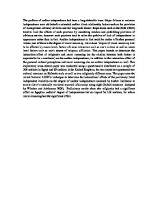
V+
_|— "m" ——
330/10
330/10
dd 3: 2006
(60) Provisional application NO- 60/406,207, ?1ed0nAug~
100
. . . ..
7 116 162
.
Flled: US. Applications:
... ... ..
FOREIGN PATENT DOCUMENTS
Related US. Patent Documents
E221; sugaotgm NO _
Kirn
1/2003 Kirn
133
DATA
V“
125 _
127 +1 131
SEPARATOR
109
101
129 PWM
103
130
121
105
"
|_____rom5\_
"0 .
_,NW
"9 12637
132
1
W
£128 120
Sign 106 J\
122/‘
13537
+
111 '
1 17
V‘YAYAY
V1‘
% é
1 18
‘M
+ ' 112
US. Patent
Mar. 27, 2012
US RE43,265 E
US RE43,265 E 1
2
REDUCED OUTPUT TOPOLOGY FOR MULTI-REFERENCE SWITCHING AMPLIFIERS
sign 106 is high, transmission gate 109 is activated, forcing the control input of switching device 126 to follow the complement of coarse pulse width stream 133, as inverted by inverter 121. Resistor 119 serves to limit output current of
differential ampli?er 1 1 1. Conversely, if the indicated sign 106 of the incoming data stream 110 is low; switching devices 127 and 128 are modu lated by the coarse pulsewidth stream 133 (throughAND gate
Matter enclosed in heavy brackets [ ] appears in the original patent but forms no part of this reissue speci?ca tion; matter printed in italics indicates the additions made by reissue.
108) and its complement (through transmission gate 110 and inverter 121), respectively. Resistor 120 serves to limit output current of differential ampli?er 112. Coarse modulation in this fashion operates exactly as shown in the multi-reference
REFERENCE TO RELATED APPLICATION
application referenced above.
This application claims priority to US. Provisional Patent
A second reference voltage, proportional to the power sup
Application Ser. No. 60/406,207, ?led Aug. 27, 2002, the entire content of which is incorporated herein by reference.
ply voltage V+, is formed by the resistor divider 123/124, and
FIELD OF THE INVENTION
turbed by transmission gate 109, switching device 125, or diode 115, differential ampli?er 111 outputs a voltage to
input to differential ampli?ers 111 and 112. When not dis
This invention relates generally to multi-reference switch
ing ampli?ers and, in particular, to a simpli?ed output topol
20
ogy associated with such ampli?ers.
with the inverse (from inverter 135) of the ?ne pulsewidth stream from pulsewidth modulator 105, forcing switching
BACKGROUND OF THE INVENTION
Multi-reference switching ampli?ers of the type shown, for example, in PCT application PCT/US99/2669l, entitled
25
modulator 105. 30
bridged con?gurations, respectively) per reference added. 35
ers.
SUMMARY OF THE INVENTION
The present invention resides in a method and attendant
When not disturbed by transmission gate 110, switching device 127, or diode 116, differential ampli?er 112 outputs a
device and one or two switching devices (for non-bridged or
Particularly in cost-sensitive applications, there remains a need for a simpli?ed output topology that retains the function and resolution inherent in multi-reference switching ampli?
device 126 to turn on, through the resultant output increase of differential ampli?er 111. This results in switching at the
output of switching device 126 between ground and the ref erence voltage formed by resistors 123 and 124, inversely modulated by ?ne-resolution 103 provided to pulse width
“Multi-Reference High Accuracy Switching Apparatus,” yield signi?cantly higher instantaneous resolution than stan dard switching ampli?ers. The cost for this performance improvement, however, resides in an additional regulatory
cause the output of switching device 126 to equal the refer ence voltage formed by resistors 123 and 124. When the indicated sign 106 is low, NOR gate 113 turns on diode 115
40
voltage to cause the output of switching device 128 to equal the reference voltage formed by resistors 123 and 124. When the indicated sign 106 is high, NOR gate 114 turns on diode 116 with the inverse (from inverter 135) of the ?ne pulse width stream from pulse width modulator 105, forcing switching device 128 to turn on, through the resultant output increase of differential ampli?er 112. This results in switch ing at the output of switching device 128 between ground and the reference voltage formed by resistors 123 and 124,
circuitry for reducing the number of regulatory and switching
inversely modulated by ?ne-resolution 103 provided to pulse
devices in a multi-reference switching ampli?er. In the pre
width modulator 105. In the discussion above, coarse-resolution data 102 is used
ferred embodiment, multiple independently-modulated
to modulate V+ on one side of load 132, while ?ne-resolution
effective references are summed at a load through use of both
linear and switched control of switching devices.
45
data 103 is used to modulate the reference voltage formed by resistors 123 and 124 on the other side of load 132, under
control of data sign 106. Although summation at the load of
BRIEF DESCRIPTION OF THE DRAWING
multiple references, modulated by appropriate resolutions, FIG. 1 shows a preferred embodiment of the present inven tion.
directly follows the technique disclosed in the multi-refer 50
plished by the present invention with signi?cantly fewer out put switching devices.
DETAILED DESCRIPTION OF THE INVENTION
Referring now to FIG. 1, switching devices 125, 126, 127, and 128 form a bridged output known in the art as an “H”
55
bridge. Inductors 129 and 130, in conjunction with capacitor 131, ?lter switching alias products from the load 132. Note that in this case only four output switching devices are used. Data separator 101 isolates coarse data 102 and ?ne data 103 from incoming data stream 100. These data streams 102 and 103 are presented as inputs to pulsewidth modulators 104 and 105, which proportionally convert said coarse data 102 and ?ne data 103 into modulated coarse pulse stream 133 and
I claim: 1. In a multi-reference switching ampli?er wherein switch ing devices control power supplied to a load in response to an
input data stream having a sign, a simpli?ed output topology,
comprising: ?rst and second independently modulated references, 60
wherein the second one of the references is derived
through a voltage divider; a data separator operative to separate the input data stream into [course] coarse-resolution data and ?ne-resolution
?ne pulse stream 134, respectively. If the sign 106 of the incoming data stream 100 is high, as indicated by data sepa rator 101, switching device 125 is modulated by the coarse pulsewidth stream 133, through AND gate 107. While the
ence application referenced above, note that this is accom
data; 65
circuitry for modulating the ?rst one of the references on one side of the load as a function of the coarse-resolution
data; and
US RE43,265 E 4
3 circuitry for modulating second one of the references on the other side of the load as a function of the ?ne resolution data.
12. The method ofclaim 1], wherein both saidacts ofoccur in response to the input data stream having a first sign, and
wherein the methodfurther comprises: modulating the second reference voltage on the?rst side of the load as afunction ofthe?ne-resolution data; and modulating thefirst reference voltage on the second side of
2. The simpli?ed output topology of claim 1, Wherein the ?rst one of the references is a supply rail.
3. In a multi-reference switching amplifier wherein switch ing devices controlpower supplied to a load, a circuit com
the load as a function of the coarse-resolution data.
prising:
13. The method ofclaim ]],further comprising converting
first and second independently modulated references, wherein the second independently modulated reference
the coarse-resolution data and the ?ne-resolution data into
respective pulsewidth modulated pulse streams. 14. The method ofclaim 1], wherein said modulating the
is derived through a voltage divider;
first reference voltage comprises switching thefirst side ofthe
a data separator operative to separate an input data stream
load between the first reference voltage and ground, and
into coarse-resolution data and?ne-resolution data; afirst circuit configured to modulate thefirst independently modulated reference on a?rst side of the load as a
wherein said modulating the second reference voltage com prises switching the second side of the load between the
function of the coarse-resolution data; and
second reference voltage and ground. 15. The method ofclaim 1], wherein said modulating the
a second circuit configured to modulate the second inde
first reference voltage comprises using the coarse-resolution
pendently modulated reference on a second side of the load as a function of the ?ne-resolution data.
4. The circuit ofclaim 3, wherein the?rst independently modulated reference comprises a supply rail.
20
data to control a switching device coupled to the first side of the load.
16. The method ofclaim 1], wherein said modulating the
second reference voltage comprises using the ?ne-resolution
5. The circuit ofclaim 3, wherein the?rst circuit and the second circuit each comprise a pulsewidth modulation cir
data to control a switching device coupled to the second side
cuit.
of the load. 1 7. A multi-reference switching amplifier configured to supply power to a load, the amplifier comprising: afirst plural ity ofswitching devices configured to couple to a first side of the load; a second plurality of switching devices configured to
6. The circuit ofclaim 3, wherein the?rst circuit is con?g ured to modulate thefirst independently modulated reference
25
on the first side of the load as a function of the coarse resolution data in response to the input data stream having a
first sign, and wherein thefirst circuit isfurther configured to modulate the second independently modulated reference on
30
couple to a second side ofthe load;
first and second independently modulated references, wherein the second independently modulated reference
the?rst side ofthe load as afunction ofthe?ne-resolution data in response to the input data stream having a second
sign.
is derived through a voltage divider;
7. The circuit of claim 6, wherein the second circuit is configured to modulate the second independently modulated reference on the second side of the load as a function of the ?ne-resolution data in response to the input data stream hav
a data separator operative to separate an input data stream 35
ing the?rst sign, and wherein the second circuit isfurther configured to modulate the first independently modulated reference on the second side of the load as a function of the coarse-resolution data in response to the input data stream
dently modulated reference as a function of the coarse 40
having the second sign. 8. The circuit ofclaim 7, wherein the?rst circuit comprises a first plurality of switching devices and the second circuit comprises a second plurality of switching devices. 9. The circuit of claim 8, wherein the data separator is further configured to couple a sign ofthe input data stream to the first and second circuits. 10. The circuit of claim 9, wherein the first and second circuits each comprise a transmission gate configured to
receive the sign ofthe input data stream, wherein each respec tive transmission gate is coupled to one of the respective switching devices, and wherein each respective transmission gate is configured to provide the coarse-resolution data to the respective switching device in response to the sign ofthe input
45
ence as a function of the coarse-resolution data and the
50
second circuit is configured to modulate the second reference as a function of the ?ne-resolution data, and wherein, in response to the input data stream having a second sign, the
first circuit is further configured to modulate the second refl erence as afunction ofthe?ne-resolution data and the second
circuit isfurther configured to modulate the first reference as
afunction ofthe coarse-resolution data. 55
19. The amplifier ofclaim 1 8, wherein the data separator is further configured to couple the sign of the input data stream to the first and second circuits.
1]. A methodfor controlling a multi-reference switching
20. The amplifier ofclaim 18, wherein the?rst and second
comprising:
circuits each comprise a transmission gate configured to 6O
data and?ne-resolution data;
receive the sign ofthe input data stream, wherein each respec tive transmission gate is coupled to one of the respective
switching devices, and wherein each respective transmission
dividing a first reference voltage to obtain a second refer
gate is configured to provide the coarse-resolution data to the
ence voltage;
respective switching device in response to the sign ofthe input
modulating the?rst reference voltage on a?rst side ofthe ofthe load as afunction ofthe?ne-resolution data.
resolution data. 18. The amplifier ofclaim 1 7, wherein, in response to the data input stream having a first sign, the first circuit is con
?gured to modulate the first independently modulated refer
ampli?er configured to supply power to a load, the method
load as a function of the coarse-resolution data; and modulating the second reference voltage on a second side
resolution data; and a second circuit coupled to the second plurality of switch ing devices and configured to modulate the second inde
pendently modulated reference as a function of the fine
data stream.
separating an input data stream into coarse-resolution
into coarse-resolution data and?ne-resolution data; a first circuit coupled to the first plurality of switching devices and configured to modulate the first indepen
65
data stream.