Logical Effort of Higher Valency Adders David Harris Harvey Mudd College 301 E. Twelfth St. Claremont, CA 91711
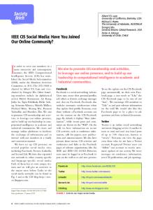
[email protected] Fig 1 Adder block diagram
Abstract – Higher valency parallel prefix adders reduce the number of logic levels at the expense of greater fan-in at each level. This paper uses the method of logical effort to evaluate the tradeoffs of higher valency for static and dynamic implementations of various adder architectures.
A4
B4
A3
B3
A2
B2
A1
B1
Cin
Precomputation G4
P4
G3
P4:4
G3:3
P3
G2
P3:3
G2:2
P2 P2:2
G1 G1:1
P1
G0
P1:1
P0
G0:0
P0:0
I. INTRODUCTION
Prefix Network
Higher valency parallel prefx adders are popular for high performance applications such as microprocessor ALUs [5, 1, 3, 4]. A valency-v N-bit adder requires O(logvN) logic levels, so a 64 bit addition requires as few as three levels of valency 4 propagate-generate gates as opposed to six levels of valency 2. However, the higher valency gates have greater logical effort and parasitic delay, are more complex to design, and are not always available in standard cell libraries. Is higher valency addition really faster? Domino gates have lower logical efforts than their static counterparts and hence can use greater fan-ins. Does this mean higher valencies are better suited to domino than static logic? This paper uses the method of logical effort to try to answer these questions. According to the logical effort model, the delays of valency-2, 3, and 4 designs are all approximately the same for a given architecture, circuit family, and wire load model. This paper closely follows the methodology of [2]. It first describes the static and domino gates used to compute generate and propagate signals for the various valencies and tabulates the estimated logical effort and parasitic delay of each gate. It then shows the prefix networks and the critical paths that were examined. Finally, it calculates the delays for valency 2, 3, and 4 for each architecture and circuit family using the method of logical effort.
G3:0
G2:0
C3
G1:0
C2
G0:0 C0
C1
Postcomputation
C4 Cout
S4
S3
S2
S1
Fig 2 Bitwise PG and sm XOR gates Inverting Static CMOS
Bitwise PG
Ai
2 Bi
2
Bi
2
Ai
2
Gi Ai
Pi Sum XOR
2 Gi-1:0
1
Gi-1:0
1
4
Footless Domino
Ai
4
Bi
4
Bi
Pi
1
φ Pi
Ai_h
1
1
2 Ai_l
2
2
Ai_h 2
Bi_h
2
2
Bi_l
φ
4
1
1
Ai_l
Pi
2
Pi
Si
Pi'
2
Gi
H
Pi
H
Ki
tiny
1
G i-1:0 4 Gi-1:0 4 G i-1:0 2 Gi-1:0 2
H
2 Pi
2
2
Pi 2
Gi-1:0
2
2
Ki-1:0
P i'
Pi'
H
Si_h
H
Si_l
Table 1 Bitwise PG and sum XOR delay estimates Cell
Term
Bitwise
LEbit PDbit LExor PDxor
Sum XOR
Noninverting CMOS 9/3 6/3 + 1 9/3 9/3 + 12/3
Inverting CMOS
Footed Domino
Footless Domino
9/3 6/3 9/3 9/3 + 12/3
6/3 7/3 3/3 7/3
4/3 5/3 2/3 5/3
* + * +
5/6 5/6 5/6 5/6
* + * +
5/6 5/6 5/6 5/6
II. LOGICAL EFFORT OF CIRCUIT BUILDING BLOCKS The three basic building blocks for an adder are the bitwise Propagate/Generate (PG) cells, the group PG cells in the prefix network, and the sum XORs, as shown in Fig 1. High performance datapath adders often build these cells from domino gates while static CMOS is preferable when design simplicity and power consumption take precedence over utmost performance. Fig 2 shows implementations of the bitwise PG cells and the sum XOR gates using static CMOS and domino gates. The static designs use propagate and generate (PG) while the domino add kill (K) for monotonic sum computation. The transistor widths are specified in arbitrary units to deliver unit drive. Noninverting static CMOS gates add an inverter after
0-7803-8622-1/04/$20.00 ©2004 IEEE
each inverting stage. Footed domino gates require an extra clocked evaluation transistor. The logical efforts (LE) and parasitic delays (PD) are given in Table 1. Prefix networks consist of black cells, gray cells, and buffers. Black cells compute both propagate and generate signals. Gray cells compute only generate, and buffers reduce the loading presented by noncritical paths. Fig 3 shows circuit implementations of propagate and generate gates for valency 2. Inverting static CMOS designs require alternating stages of the gates shown and their DeMorgan complements that accept inverted inputs and produce true outputs. [2] found that the difference in delay of the complementary stages is insignificant, so it will be ignored.
1358
Fig 3 Valency 2 static and dynamic generate/propagate gates G0
4 P1 G1
G1
4
4
1 G0
2
P1
2
Gi:j
P1
2 P0
2
P1
2
P0
2
φ
1
1
1
P1:0 G0 G1
2
1
P0 2
K0 2
2
P1
K1
Fig 5 Valency 2 adder architectures
H
G1:0
H
P1:0
H
K1:0
(c) Brent-Kung 15
14 13
12
15:14
13:12
Fig 4 Valency 4static and dynamic generate/propagate gates P1 P3
4 G2
G3
8
G2 G3
1 P3
4 G1
8 G0
9
8
7
6
5
4
3
2
1
0
9:8
7:6
11:8
5:4
3:2
7:4
15:8
1:0
3:0
7:0
8
8
φ
8
G1 2 P2
10
11:10
15:12
P2
11
1
G0 2 P1
4
G3:0
G0 G1
4
G2 4/3
4
G3
4
1
2
1
1
1
4P0 P1
4 K0
4
4
P2
4
P3
4
G3:0 P3:0
11:0
K3:0 K1
13:0
9:0
5:0
2 K2
4/3 K3
15:014:0 13:0 12:0 11:0 10:0 9:0 8:0 7:0 6:0 5:0 4:0 3:0 2:0 1:0 0:0
1
(d) Sklansky
P3 P P1 2 P0
P3:0
15
14 13
12
11
10
9
8
7
6
5
4
3
2
1
0
Table 2 Gray and black cell delay estimates 15:14
Valency
Term
2
PDg PDp LEg1 LEg0 LEp1 LEp1 LEp0 PDg PDp LEg2 LEg1 LEg0 LEp2 LEp1 LEp2 LEp1 LEp0 PDg PDp LEg3 LEg2 LEg1 LEg0 LEp3 LEp2 LEp1 LEp3 LEp2 LEp1 LEp0
3
4
Cell
Inverting CMOS 7/3 2
Gray Black Black 13/3 3
Gray Gray Black Black Black 17/3 4
Gray Gray Gray Black Black Black Black
Noninverting CMOS 7/3 + 1 2+1 5/3 6/3 6/3 10/3 4/3 13/3 + 1 3+1 7/3 8/3 9/3 5/3 9/3 10/3 14/3 5/3 17/3 + 1 4+1 9/3 10/3 10/3 12/3 8/3 6/3 12/3 14/3 12/3 18/3 6/3
Footed Domino 6/3 + 5/6 3/3 + 5/6 1/2 * 5/6 3/3 * 5/6 3/3 * 5/6 6/3 * 5/6 3/3 * 5/6 10/3 + 5/6 4/3 + 5/6 4/9 * 5/6 2/3 * 5/6 4/3 * 5/6 4/3 * 5/6 4/3 * 5/6 8/3 * 5/6 8/3 * 5/6 4/3 * 5/6 13/3 + 5/6 5/3 + 5/6 5/12 * 5/6 5/9 * 5/6 5/6 * 5/6 5/3 * 5/6 5/3 * 5/6 5/3 * 5/6 5/3 * 5/6 10/3 * 5/6 10/3 * 5/6 10/3 * 5/6 5/3 * 5/6
Footless Domino 4/3 + 5/6 2/3 + 5/6 1/3 * 5/3 2/3 * 5/6 2/3 * 5/6 4/3 * 5/6 2/3 * 5/6 7/3 + 5/6 3/3 + 5/6 1/3 * 5/6 ½ * 5/6 3/3 * 5/6 3/3 * 5/6 3/3 * 5/6 6/3 * 5/6 6/3 * 5/6 3/3 * 5/6 10/3 + 5/6 4/3 + 5/6 1/3 * 5/6 4/9 * 5/6 2/3 * 5/6 4/3 * 5/6 4/3 * 5/6 4/3 * 5/6 4/3 * 5/6 8/3 * 5/6 8/3 * 5/6 8/3 * 5/6 4/3 * 5/6
13:12
11:10
15:12 14:12
15:8
9:8
7:6
11:8 10:8
14:8
13:8
5:4
7:4
3:2
6:4
1:0
3:0
2:0
12:8
15:014:0 13:0 12:0 11:0 10:0 9:0 8:0 7:0 6:0 5:0 4:0 3:0 2:0 1:0 0:0
(e) Kogge-Stone 15
14 13
12
11
10
9
8
7
6
5
4
3
2
15:14 14:13 13:12 12:11 11:10 10:9
9:8
8:7
7:6
6:5
5:4
4:3
3:2
2:1
15:12 14:11 13:10
3:0
2:0
15:8
14:7
13:6
12:9
11:8 10:7
9:6
8:5
7:4
6:3
5:2
4:1
12:5
11:4 10:3
9:2
8:1
7:0
6:0
5:0
4:0
1
0
1:0
15:014:0 13:0 12:0 11:0 10:0 9:0 8:0 7:0 6:0 5:0 4:0 3:0 2:0 1:0 0:0
(f) Han-Carlson 15
14
13
12
11
10
9
8
7
6
5
4
3
15:14
13:12
11:10
9:8
7:6
5:4
3:2
15:12
13:10
11:8
9:6
7:4
5:2
3:0
15:8
13:6
11:4
9:2
7:0
5:0
2
1
0
1:0
15:0 14:0 13:0 12:0 11:0 10:0 9:0 8:0 7:0 6:0 5:0 4:0 3:0 2:0 1:0 0:0
Similarly, Fig 4 shows the circuit designs for valency 4. Table 2 gives the logical efforts and parasitic delays for the various inputs to black and gray cells in each circuit family. III. ADDER ARCHITECTURES Adders are distinguished by the arrangement of cells in the group PG logic. Fig 5 shows typical parallel prefix architectures for valency 2 gates [6]. One of several paths may be most critical depending on the cell delays; the black highlighted lines indicate the path that was assumed to be critical in this study. Similarly, Fig 6 shows the analogous architectures for higher valency 3. Higher valency adders offer a number of hybrid tree / select architectures such as the spanning tree and sparse tree that reduce the number of cells in the parallel prefix network in exchange for adding short ripple networks; these variants are not considered in this study.
(g) Knowles [2,1,1,1] 15
14
13
12
11
10
15:14 14:13 13:12 12:11 11:10 10:9
15:12 14:11 13:10
15:8
14:7
13:6
9
8
7
6
5
4
3
2
9:8
8:7
7:6
6:5
5:4
4:3
3:2
2:1
12:9
11:8 10:7
9:6
8:5
7:4
6:3
5:2
4:1
3:0
2:0
12:5
11:4 10:3
9:2
8:1
7:0
6:0
5:0
4:0
1
0
1:0
15:0 14:0 13:0 12:0 11:0 10:0 9:0 8:0 7:0 6:0 5:0 4:0 3:0 2:0 1:0 0:0
(h) Ladner-Fischer 15
15:14
14
13
13:12
15:12
12
11
11:10
10
9
9:8
11:8
15:8
13:8
15:8
13:0
8
7
7:6
5
5:4
7:4
7:0
11:0
6
4
3
3:2
2
1
0
1:0
3:0
5:0
9:0
15:0 14:0 13:0 12:0 11:0 10:0 9:0 8:0 7:0 6:0 5:0 4:0 3:0 2:0 1:0 0:0
1359
IV. LOGICAL EFFORT DELAY MODEL
V. RESULTS
The method of Logical Effort provides a simple method for determining a lower bound on critical path delay in circuits with negligible wire capacitance. If the path has M stages, a path effort of F, and a parasitic delay of PD, the delay (in τ) achieved with best transistor sizes is
The adder delays were evaluated using a MATLAB script. Fig 7 plots delay (in FO4 inverter delays) vs. number of bits for various adder architectures, and circuit families assuming w = 0.5. The three curves on each set of axes indicate valency 2, 3, and 4 delays. The delay is nearly independent of the valency for both static and domino designs of most architectures. Brent-Kung architectures are an exception that benefit from higher valency for noninverting circuits because the stage effort is too low with valency 2, but Brent-Kung is not the fastest architecture in any case. Domino gates are consistently faster than static and footless domino is faster than footed. The designs with two gates per stage (all but inverting CMOS) are better at driving the heavy wire loads and hence perform better for wide adders.
D = DF + PD = MF 1/ M + PD
(1)
where D is measured in units of τ, the delay of an ideal inverter with no parasitic capacitance driving an identical inverter. Delay is normalized to that of a fanout-of-4 inverter with the conversion 1 FO4 ˜ 5 τ. In general, achieving least delay requires using different transistor sizes in each gate (although this delay model has assumed that all transistors in a branch scale uniformly). A regular layout with consistent transistor sizes in each type of cell is easier to build but may sacrifice performance. Consider designing all cells to have an arbitrary unit drive (i.e. output conductance). Define an inverter with unit drive to have unit input capacitance. For circuits with a single stage per cell (e.g. inverting static CMOS), the path effort delay is simply the sum of the effort delays of each stage: M
DF = ∑ f i
(2)
i =1
The total delay is still the sum of the path effort and parasitic delays. In a circuit with two stages per cell (e.g. noninverting static CMOS or domino), let us design the first stage to have unit drive. Choose the size of the second stage for least delay. If the path has C = M/2 cells and the effort of the ith cell is Fi, the path effort delay is C
DF = ∑ 2 Fi
VI. CONCLUSIONS The logical effort model facilitates rapid comparison of a wide variety of adder architectures using multiple circuit families while accounting for the costs of fanout and interconnect. Under the assumptions made in this paper, the delay is nearly independent of the valency for both static and domino designs of most architectures. Brent-Kung architectures are an exception that benefit from higher valency for noninverting circuits because the stage effort is too low with valency 2, but Brent-Kung is not the fastest architecture in any case. Valency 2 designs are the simplest to implement. This paper has not considered the area, power, or wiring tradeoffs of higher valency adders. In practice, the logical efforts of gates are likely to be lower on account of velocity saturation, but the parasitic delays are likely to be higher when internal nodes are considered. Simulations of extracted layouts could answer these questions.
(3)
REFERENCES
i =1
[2] showed that the delay with uniform sizes is only slightly longer than the delay with arbitray sizes except on architectures like Sklansky that have unusually large fanouts on certain nodes. The uniform size designs are also easier to layout and permit closed-form results when wire capacitance is considered, so we focus on them in this paper. Horizontal wires add capacitance to the load of each stage. Let the wire capacitance be w units per column spanned. w depends on the width of each column, the width and spacing between wires, and the size of a unit transistor; in a trial layout in a 180 nm process, w ˜ 0.5. While there is no closed-form solution for the minimum-delay problem with wire capacitance, the delay assuming fixed cell sizes is readily calculated by adding the wire capacitance to the stage effort fi or Fi in EQ (2) or (3).
1
A. Beaumont-Smith and C. Lim, “Parallel prefix adder design,” Proc. 15th IEEE Symp. Comp. Arith, pp. 218-225, June 2001. 2 D. Harris and I. Sutherland, “Logical effort of carry propagate adders,” Proc. 37th Asilomar Conf. Signals, Systems, and Computers, pp. 673-678, 2003. 3 T. Lynch and E. Swartzlander, “A spanning tree carry lookahead adder,” IEEE Trans. Computers, vol. 41, no. 8, Aug. 1992, pp. 931-939. 4 S. Mathew, M. Anders, R. Krishnamurthy, and S. Borkar, "A 4-GHz 130-nm address generation unit with 32-bit sparse-tree adder core," J. Solid-State Circuit, vol. 38, no. 5, May 2003, pp. 689-695. 5 S. Naffziger, “A subnanosecond 0.5 µm 64b adder design,” Intl. Solid-state Circuits Conf., 1996, pp. 362-363. 6 N. Weste and D. Harris, CMOS VLSI Design, Addison-Wesley, 2005.
1360
Fig 6 Valency 3 adder architectures
(a) Brent-Kung 26
25
24
23
22
21
20
19
18
17
16
15
14
13
12
11
10
9
8
7
6
5
4
3
2
1
0
26:0 25:0 24:0 23:0 22:0 21:0 20:0 19:0 18:0 17:0 16:0 15:0 14:0 13:0 12:0 11:0 10:0 9:0 8:0 7:0 6:0 5:0 4:0 3:0 2:0 1:0 0:0
(b) Sklansky 26
25
24
23
22
21
20
19
18
17
16
15
14
13
12
11
10
9
8
7
6
5
4
3
2
1
0
26:0 25:0 24:0 23:0 22:0 21:0 20:0 19:0 18:0 17:0 16:0 15:0 14:0 13:0 12:0 11:0 10:0 9:0 8:0 7:0 6:0 5:0 4:0 3:0 2:0 1:0 0:0
(c) Kogge-Stone 26
25
24
23
22
21
20
19
18
17
16
15
14
13
12
11
10
9
8
7
6
5
4
3
2
1
0
26:0 25:0 24:0 23:0 22:0 21:0 20:0 19:0 18:0 17:0 16:0 15:0 14:0 13:0 12:0 11:0 10:0 9:0 8:0 7:0 6:0 5:0 4:0 3:0 2:0 1:0 0:0
(d) Han-Carlson 26
25
24
23
22
21
20
19
18
17
16
15
14
13
12
11
10
9
8
7
6
5
4
3
2
1
0
26:0 25:0 24:0 23:0 22:0 21:0 20:0 19:0 18:0 17:0 16:0 15:0 14:0 13:0 12:0 11:0 10:0 9:0 8:0 7:0 6:0 5:0 4:0 3:0 2:0 1:0 0:0 (e) Ladner-Fischer 26
0
26:0
0:0
1361
30
30
30
20
20
20
20
10
10
10
10
0 0 30
Sklansky
60 80
0 0 30
20 40 60
80
0 0 30
20
40
60 80
0 0 30
20
20
20
10
10
10
10
20 40
60 80
0 0
20 40 60
80
0 0
20
40
60 80
0 0
30
30
30
30
20
20
20
20
10
10
10
10
0 0 Kogge-Stone
20 40
20
0 0
20 40
60 80
0 0
20 40 60
80
0 0
20
40
60 80
0 0
30
30
30
30
20
20
20
20
10
10
10
10
0 0 Han-Carlson
Delay (FO4)
Ladner-Fischer
Brent-Kung
Fig 7 Adder delay vs. # of bits (logical effort model results)
30
20 40
60 80
0 0
20 40 60
80
0 0
20
40
60 80
0 0
30
30
30
30
20
20
20
20
10
10
10
10
0 0
20 40 60 80 Inverting CMOS
0 0
20 40 60 80 Noninverting CMOS
0 0
# of bits
20 40 60 80 Footed Domino
0 0
Valency 2 Valency 3 Valency 4
1362
20 40
60 80
20 40
60 80
20 40
60 80
20 40
60 80
20 40 60 80 Footless Domino