Logical Effort of Carry Propagate Adders David Hanis and Ivan Sutherland Harvey Mudd College / Sun Microsystem Labratones 301 E. Twelfth S t Claremont, CA 9171 1 David €IanislZ!hnic.eduI Ir~an.Sutherland@suuconi Abstract - A wide assortment of carry propagate adders offer varying areadelay tradeoff% Wiring and choice of circuit family also afiect the size and performance. This paper uses the method of Logical Effoort to characterize the effects of architecture, circuit family, and wire capacitance on adder delay. Domino logic offers about a 30% speedup on most valency-2 adders. Although KoggeStone adders are fastest in the absence of wire, other architectures such as variants on the Sklansky adder offer regular layouts and better delay in the presence of wiring capacitance.
I. I~TRODUCIION Fast adders are widely used in CMOS circuit design. The literature describes many adders including ripple carry, carry loo~~canyselect[2],canyskip[12],carryincrement[16, 181, Sklansky (conditional sum) [14], Brent-Kung [3], KoggeStone [IO], Ladner-Fischer [l I], Han-Carlson [7], and Knowles [9]. Each mhitecture offers different tradeoffs between delay, area, and wiring complexity. Analyhcal delay models help designers evaluate these tradeoffs, but simply counting logic levels is inadequate because circuit delay also depends on fanout and wire capacitance. Huang and Ercegovac [SI used an RC delay model to evaluate the effect of architecture and wiring capacitance on the Sklansky, KoggeStone, and Knowles adder architectures. The method of Logical Effort [151builds on the RC delay model to offer a convenient shorthand for understanding the effects of fanout and gate sizing on delay. Dao and Oklobdfja [5,6] applied this method to a few adders and concluded that logical effort predicted absolute delays within 5-20% of HSPICE. This paper applies logical effort to understand the delay of eight different adder architectures that canbe expressed as prefut computations according to the notation of [17]. The results show how adder delay depends on the number of inputs, the adder architectures, the cost of interconnect, and the circuit style. The model shows that most adder architectures can use uniform gate sizes to achieve regular layout with negligible performance loss. An exception is the Sklansky architectme that has highly irregular fanouts. This leads to a proposal for "helpei' gates to construct very fast adders with regular layouts and low wiring cost
n. LOGICAL EFFORTOF CIRCTJl" BUILDING BLOCKS The three basic building blocks for an adder are the bitwise Propagate/Gmerate (PG) cells, the group PG cells, and the sum XORs. High pehmance datapath adders often build these cells h m domino gates while static CMOS is preferable when
0-7803-8 104-1/03/$17.00 02003 IEEE
873
design simplicity and power consumption take precedence over utmost performance. Static CMOS bitwise gates will compute generate as Cj = A; * B, and propagate as Pi = A ; + B,. The sum is computed as Si= (A, B, ) G, l a . Domino designs require monotonic inputs to the sum XOR This is best done by calculating bitwise and group kill signals (K) and using XOR for propagate so that P,G, and Kare l-of-3 hot. D e h e the group PG cell input coming 6om hits i:k as the upper input and that &omk-1j as the lower input There are two types of group PG cells. Following the notation of [4], we call the cells black cells and gray cells. Black cells compute both C, and Pj,as defined in EQ (3). Gray cells compute only Cil. Black cells are required when the cell output drives the upper input of another group PG cell. The simpler gray cell may be used when the output drives only lower inputs or sum logic. Consider four circuit styles: noninvehg static CMOS, inverting static CMOS, footless domino, and footed domino. Fig 1 shows the basic cell designs. Inverting static CMOS gates consist of a single stage of logic for each cell (except that the final XOR requires an input inverter). Alternating stages use alternating polarities of inputs and outputs. Black cells contain both the group G and P gates while gray cells have only the G gate. Noninverting static CMOS gates add an output inverter to the bitwise and goup static gates. Therefore, only the ANDOR and AND funaions are required for group G and P, respectively. Footless domino gates computing I-of-3 hot P,G, and K signals are shown in the second column. Each consists of a dynamic gate followed by an HI-skewinverter. Keepers and secondary precharge bansistors are not shown. The group logic is shown for a black cell; a gray cell omits the P output In the domino design, K, ,? = G, 1o so monotonic me and complementary versions of the carry signals are available at each finalXOR Footed domino gates are identical except for an extra series clocked evaluation transistor and greater transistor widths to compensate. Transistors are annotated with widths measured in arbifmry units so that each pulldown stack has unit effective resistance. Table 1 lists the logical effort and parasitic delay of each cell input for each circuit family. The logical effoa LE is the ratio of the input capacitance of the gate input to the input capacitance (3 units) of an inverter with the same unit effective resistance. The parasitic delay PD is estimated by counting the total transistor width on the output node,
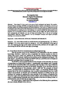
Adders are distinguished by the arrangement of cells in the group PG logic. Fig 2 shows eight such architectures for?+16.
The upper box contains the bitwise PG logic and the Tnhle 1 L q i d effort nad pvasitic delay of adder -t
assuming diffusion and gate capacitance are approximately equal. In domino and noninverting static CMOS circuits, the output inverter also contriiutesparasitic delay. LE and PD are used in place of the usual symbols g and p to avoid confusion with generote and propogate. Notice that the black cell has four inputs: G,r, Gk.lJ,P,h and Pk~l,: These are denoted as the upper and lower generate and propagate signals, gu,gl, pu, and pl, respectively, and each has a Merent logical effort For inverting static CMOS circuits, the logical effort and parasitic delay are the average of the two polarities'. Some paths through the static XOR gate involve only a single A2201 stage while others also involve the inverter. A conservative estimate calculates the logical effort for the single stage path based on the 9 units of input capacitance on the G input. The parasitic delay is largest for the two-stage path, consisting of 9/3 for the inverter to drive its own diffusion parasitics and gate capacitance of the second stage plus 1U3 for the diffusion m i t i c s on the second stage. In certain cases,buffers reduce the capacitance presented by noncritical f o h of the circuit. Assume these buffers have half the drive (twice the resistance) of an ordinary gate and hence half the input capacitance. For the purpose of branching, the buffers therefore contribute only half the capacitance of a gate with comparable logical effort
If all cell sizes are chosen to provide unit drive as will be done in Section 4, this gives the correct delay through the path. If some cell sizes are selected for minimum delay, the logical efforts should be the geometric means of the efforts of the two polarities. In this case, the average and geometric mean are nearly identical, so the distinction is unimportant.
874
bkks
lower box contains the s u m logic. In the middle, the prefix tree is built &om black cells, gray cells, and white buffers. The vertical axis indicates logic level and the critical path is indicated with a heavy line. For example, the ripple cany adder in Fig 2a is slow for long additions because the critical path propagates through N-1 gray cells. The critical path of each adder is described in more detail in Table 2. Each row of the table corresponds to the delay of a cell. The delay bas three components: an effort delay F based on the size of the load, a parasitic delay P based on the cell itself, and wire delay based on the length of the horizontal wires between cells (measured in columns traversed). For example, the ripple carry adder path begins with inputs coming &oma previous unit; these inputs see loading 60x11the bitwise PG cells (LEb,,)but their parasitic delay is not parl of the adder delay. Then the PIsignal is computed and drives the upper propagate input of a gray cell. The generate antput of this cell in tum drives the lower generate input of the next cell and as well as the associated sum XOR. This repeats N-1 times. Note that the final gray cell must drive both the SI6 XOR and the Cd gray cell, so the load is the same as on the other gray cells. Finally, the sum XOR contributes a parasitic delay. The effort delay driving the next unit is not counted because an effort delay was already allocated on the ptinmy inputs. Several simplifying assumptions have been made: ,411 inputs amivi at the same time with eq~aldrive. Only horizontal wires are counted in the wire load. Vedcal wires are assumed to be short enough to neglecl (or lump into the parasitic gate delay). The A, B, term used to compute the final sum is not explicitly shown and may use Mered versions of the inputs to contriiute negligible loading. Wires are assumed to be short enough that only capacitance must be considered, not wire RC delay. This assumption is suppad by [SI.
Note that in the Brent-Kung and Han-Carlson architecturesthere is never more than one black or gray cell per pair of bits in any given row. If pipelining is not required, the adder may be condensed to half the width, shortening the lateral wires as indicated in the table. Fi 2 Adder architedurej (a) Ripple Carry 1 0 9
8
7
6
5
4
(d) Sklansky
(
L42!
150140130120
3 1 0 0 9 0 6 0 7:0 6:O 5 0 4 0 L..
(b) Carry Increment (f) HanCadson
In most of the adder architectures, the stage effort is fairly constant throughout the adder if wire capacitance is neglected We will see that this means uniform gate sues may be used throughant with very little loss in performance. In the Sklansky graph, the fanout increase exponentially along the critical path. This leads to very poor performance unless cells have greater drive. One means to provide greater drive is to use larger gates in specific locations, but this increases the number of cells to design and verify and leads to irregular layout. When trains must climb a steep grade with a heavy load, multiple locomotives are linked together. The extra locomotives are called hebers. In the Sklansky graph, multiple cells may be linked together to provide more current to drive the large fanouts and long wires. Four such adders with helpers are shown in Fig 3. Each is based on the Sklansky architecture. They differ in the number of columns required and the space available for buffers in pipelined adders.
875
(h) Ladner-Fischer
IV.LQGICAL EFFORTDELAYMODEL The method of Logical Effort provides a simple method for determining a lower bound on critical path delay in ckui& with negligible wire capacitance. If the path has Mstages, a path effort of F, and a parasitic delay of PD, the delay (in ) achieved with best transistor sizes is D = D, +PD = m"*' + PD
(1)
where D is measured in units of ,the delay of an ideal inverter with no parasitic capacitance driving an identical inverter. Delay is often normalized to that of a fanout-of-4 inverter with the conversion 1 F04 5 . In a 180 nm pmess, 1 F 0 4 60 ps. To illustrate the delay model, consider an N=4-bit ripple cany adder. According to the data from the previous sections the least delay is given below. Note that the inverting design is faster because the extra inverters in the noninverting CMOS version.
-
Flg3 Helperaddem
-
Inverting cntos: M =N+1=5 F = &Ebn)&Ew)&Ed+ LE&)' = (9/3)(6/3)(6/3 + 913)' = 750 DF = 5(750)'" = 18.8 PD = PI& + 3PD, + PD,, = (6/3) + 3(7.5/3) + (9/3 + 12/3) = 16.5 = 18.8 + 16.5 = 35.3 = 7.1 F04 D Noninverting CMOS: M =2(N+1)=10 F =&EdJ-Em&Em+ Ed3 = (9/3)(6/3)(6/3 + 9/3)' = 750 DF = 10(750)1''0= 19.4 PD = P&1+ 3PDm + PD, = (6/3 +1) + 3(7B + 1) + (9/3 + 12/3) = 20 D = 19.4 + 20 = 39.4 = 7.9 F 0 4 In general, achieving least delay requires using different transistor sizes in each gate (although this delay model has assumed that all transistors in a branch scale uniformly). A regular layout with consistent transistor sizes in each tyQe of cell is easier to build but may sacrifice performance. Consider designing all cells to have an arbitmy unit drive (i.e.output conductance). Define an inverter with unit drive to have unit input capacitance. For circuits with a single stage per cell (e.g. inverting static CMOS), the path effort delay is simply the sum of the effort delays of each stage:
f;
D,=
(2)
i=l
The total delay is still the sum of the path effort and parasitic delays. In a Cbit ripple cany adder built frmn inverting static CMOS gates the delay is
876
Inverling CMOS D,r = LEb, +LEw + 3 @ E w + L L ) = 913 + 613 + 3(6/3 + 913) = 20 D = 20 + 16.5 = 36.5 = 1.3 F04
In a circuit with two stages per cell (e.g. noninverting static CMOS or domino);let us design the firststage to have unit drive. Choose the size of the second stage for least delay. If the path has C = M2 cells and the effortof the ithcell is F,, the path effort delay is DF =
2&
(3)
i-,
In a 4bit ripple carry adder built from noninverting static CMOS gates the delay is
=2fi+
+3
2fi
.
2
m
=19.7~
D
=
19.7 + 20 = 39.1 = 1.9 F04
These delays are only slightly slower than ideal, justifying the use of a regular layout. The two-stage cell delay estimate is optimistic because in a regular design the second stage size will be fixed for each cell. However, the results iknn the singlestage cell estimate suggest the penalty is not large. Horizontal wires add capacitance to the load of each stage. Let the wire capacitance be w units per column spanned. w depends on the width of each column, the width and spacing between wires, and the sue of a unit transistor; in a hial layout in a 180 nm process, w 0.5. While there is no closed-form solution for the minimumdelay problem with wire capacitance, the delay assuming fxed cell sues is readily calculated by adding the wire capacitance to the stage effortJ or F, in EQ (2) or (3).
-
v. RESULTS The adder delays were evaluated using a MATLAB script Table 3 lists delay (in F04 inverter delays) for various adder architectnres and widths assuming no wire capacitance and inverting static CMOS cells. It compares the delay achieved using best transistor sizes with the delay using uniform cell sizes. Observe that the penalty for uniform cell sizes is small in all cases except cany increment and Sklansky (where the fanouts vary wildly from one stage to another). This justifies using uniform cell sizes for most adders and for employing helpers on the Swansky architecture to drive the high fanouts. The remaining results are based on uniform cell sizes. Table4 evaluates the effect of adder size by listing the delay of inverting static CMOS and fwted domino adders assuming Wiring capacitance d . 5 . Table 5 evaluates the impact of effect of circuit family, again assuming d . 5 . Table6 evaluates
the impact of wire capacitance on inverting static CMOS adders. The KoggeStone, Han-Carhn, and Knowles adders require a large number of parallel wiring backs for wide adders. This generally entails packing the wires close together, increasing the coupling capacitance on each wire. Huang and Ercegovac [SI found tbk nearly doubles the wire capacitance; therefore these architectures may be evaluated using the w1.O column of Table 6 compared against the ~ 0 . column 5 for adders with fewer wires. The critical paths of most architectures (excluding Kogge Stone, Han-Carlson, and Knowles) pass through a series of gray cell lower generate inputs. These adders may be sped up with asymmekic gray cells that reduce the logical effort LEd at the expense of the other inputs [15]. This provides on average 9% speedup on the footed domino circuits, but almost none on the static CMOS circuits where noncritical transistors must be enlarged to preserve unit drive and thus increase parasitic delay.
VI. CONCLUSIONS The logical effort model facilitates rapid comparison of a wide variety of adder architectures using multiple circuit families while accounting for the costs of fanout and interconnect. The Sklansky architecture is slowed by its high fanout along the critical path. This may be addressed at the expense of regularity by using larger gates along the path The helper architectures proposed in this paper gang together multiple cells to drive the high fanout nodes while maintaining regularity. Regular designs with unit drive work well in architectures with relatively constant stage efforts, i.e. all except S!&nsky and cany increment In the absence of wiring capacitance, the Kogge-Stone adder is fastest because of its low number of stages and low fanout When intef~onnectis considered, the HanCarlson and helper adders become most amactive. HanCarlson requires only half the number of columns,while helper adders are slightly faster at driving the long wires, especially when coupling capacitance is considered. Fast static CMOS adders have a delay ofabout 10,12, 14.5, and 11 F04 for 16,32,64, and 128-bit widths, respectively. Most adders have a relatively low stage effort so the footed domino designs are only about 30% faster than the inverting static CMOS architectures because the high drive capability of domino is not fully exploited This suppats the use of higher-valency [11 domino designs. Asymmetric domino gates achieve another 9% speedup. Inverting static CMOS gates are also slightly faster than their noninverting counterparts except where high fanout capability is needed; however, the difference is much smaller than a method of “counting logic levels” would predict The delays estimated h m logical effort are in good
agreementwiththeHSPICEresultsof[I],[S],and[9]. However, the best &bit footless domino adder delays of 9-10
18 R Zimmermarm, ‘Won-heuristic optimization and synthesis of parallelprefix adders,” Proc. Inti. Workshop on Logic m d
FC4 are s!ill distinctly longer than the 7 F04 delays achieved by the NaEziger domino Ling adder [13]. The differences may be amibuted to the fact that velocity sahmtion makes tall domino gates slightly faster than simple logical effm models +a, the use of valency4 cells and asymmekic gates biased to favor the critical path, and the logic level saved with the Ling algorithm. The hction of the delay amibuted to wires is important but significantly less than in [SI because this study assumed layouts with larger input transistors and a narrower column pitch to reduce the impact of wire capacitance.
Architecture$Whe.vb, pp. 123-132,Grenoble, France, Dec. 1996. TpMp 3 Add- delays: 4 invertingstzalic CMOS
REFERENCES
A Beaumont-Smith and C. Lm, “Parallel prefix adder design,” Proc,IShLEEE Symp. Comp. Arith, pp. 218-225,June 2001. 0 . B&j, “Cany-select adder,” IRE Tram.EIecrronic Computers, “01 .~ FC-I 1 lime 1962~ ~ .nn- 340.346 , ~~.~ ~
R Brent and H. Kung, “A regular layout for parallel adders,” IEEE Tram. Commtem. . .vol. G 3I. no. 3, OD. 260.264, March 1982. N. Bmgess, ‘‘Accelerated &-&p adders with low hardware cost,” P m .35“ Asiiomzr Conf Signals, System, and Computers, vol. 1,pp. 852-856,2001. H . Dao and V. Oklobdzija, “Application of logical effofion delay anaiysis of W i t static cany-lookahead adder,” Proc. 3rh AsiIomm Conf SignaLr. Systems, and Computers,vol. 2, pp. 13221324,2001. H . Dm and V. Oklobdnj’a, “Application of logical effat techniques for speed optimization and analysis of representative adders,” Proc. 35’* Adomar Conf Signals. System, and Commfem.vol. 2, m. l666-l669,2001. T.H a and D. cWi&T& --efficient VLSI addas:’ h c . f h S p p . Comp. Arith.,pp. 49-56, Sept. 1987. Z. Hung and M. Ercego~c, ‘‘Effectof wire delay on the design of prefix adders in deep submicron techno~ogy,”PTOC MhAsi/omar COI$ SignaIs, Syztem, and Computers, vol. 2, pp. 1713-1717, 2ooO. S. Knowles, “A family of adders,” Proc IEEE Symp. C o q . Arch., 1999 reprinted with comedons m Proc. I f hIEEE S p p .
Comp.Arith.,pp. 277-281, June 2001. IO P. Kogge and H . Stone, “A parallel algorithm for the eficient solution of a general class of recwence relations,” IEEE Trans. Computers,vol. G 22, no. 8, pp. 786-793, Aug. 1913. I 1 R Ladner and M. Fischa, “Parallel prefix computation:’ J. ACM, vol. 27,no.4,pp. 831-838,Oct 1980. 12 M. L e h and N. Burla, “Skip techniques for high-speed cany propagation in binary arithmetic units,” IRE Tram. EIefron Computers,EC-IO, Dec. 1962,pp. 691698. 13 S.Naf€ziger, “A subnanosecond 0.5 m 64b adder design,” Inll. S0lid;rtate Circuis Con?,1996,pp. 362-363. 14 J. Sklansky, “Conditional-sum addition logic,” IRE Trans. EIecfronic Coiputing,vol. EC-9, June 1960,pp. 226-231. 15 I. Sutherland, R Sproull, and D. Harris, Logical Effori, San Francisco: Morgan Kaufinann publishers, 1999. 16 A. Tyagj, “A reduced-area scheme for cany-select adders,” IEEE Tram. Commfers. . .vol. 42. no. IO. OD. 1162-1170,0ct 1993. 17 N. Weste and D. Harris,’CMOSLTkSIDesign.Addison-Wesley,
2004.
878
Table4 Adderdolpys:~.S;uni(omc&shp
Table 5 Adds
~ 0 . 5 uniform ; cell sire (I) Inverting CMOS, (2) NoniavertingCMOS,
(3) F w t d Domina, (4) Foodess Domino