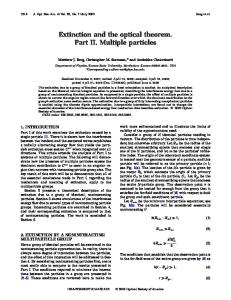
APPLIED PHYSICS LETTERS 90, 181122 共2007兲
Optical characteristics of a-plane InGaN / GaN multiple quantum wells with different well widths T. S. Ko,a兲 T. C. Lu,b兲,c兲 T. C. Wang, M. H. Lo, J. R. Chen, R. C. Gao, H. C. Kuo,b兲,d兲 and S. C. Wang Department of Photonics and Institute of Electro-Optical Engineering, National Chiao Tung University, 1001 Ta Hsueh Rd., Hsinchu, 30050 Taiwan, Republic of China
J. L. Shen Physics Department, Chung Yuan Christian University, Chung-Li, 32023 Taiwan, Republic of China
共Received 22 January 2007; accepted 10 April 2007; published online 3 May 2007兲 a-plane InGaN / GaN multiple quantum wells of different widths ranging from 3 to 12 nm were grown on r-plane sapphire by metal organic chemical vapor deposition for investigation. The peak emission intensity of the photoluminescence 共PL兲 reveals a decreasing trend as the well width increases from 3 to 12 nm. Low temperature 共9 K兲 time-resolved PL study shows that the sample with 3-nm-thick wells has a better optical property with a fast exciton decay time of 0.57 ns. The results of cathodoluminescence and micro-PL scanning images for samples of different well widths further verify the more uniform and stronger luminescence intensity distribution observed for the samples of thinner quantum wells, indicating that the important growth parameters for a-plane InGaN / GaN multiple quantum wells could be dominated by the In fluctuation and crystal quality during the epitaxial growth. © 2007 American Institute of Physics. 关DOI: 10.1063/1.2735935兴 During the past few years, group III nitrides have attracted a great amount of attention because of their application in electronic and optoelectronic devices.1–3 However, the wurtzite nitride materials exist polarization electrostatic fields along the polar c direction that result in the spatial separation of electron and hole wave functions within quantum wells and induce the quantum confined Stark effect.4 Therefore, to overcome the built-in electric field is one of main challenges for improvement of light efficiency. Recently, to eliminate such polarization effects, growth along ¯ 0兴 a-plane nonpolar orientations has been explored for 关112 ¯ ¯ 0兴 GaN on 关1012兴 r-plane sapphire and a-plane SiC, and 关101 5,6 m-plane GaN on 关100兴 LiAlO2 substrates. The optical characteristics of c-plane InGaN / GaN multiple quantum wells 共MQWs兲 have been studied intensively.7,8 Chakraborty et al. had also investigated the effect of defect density on optical properties by comparing growth on high-defect and low-defect laterally epitaxial growths.9 However, the optical properties of a-plane InGaN / GaN MQWs are still worth investigating for assistance of fabrication due to the lack of the internal field and possible different growth parameters. Since the interface roughness and treading dislocations in a-plane heterostructures are more complicated than those in c-plane heterostructures,10 the luminescence mechanism requires further clarification of the dependence of the optical characteristics on the different InGaN / GaN quantum well widths. Craven et al. had investigated optical characteristics of GaN / AlGaN MQWs with different well widths;11 however, the issues related to well width dependence of a-plane InGaN / GaN MQWs that include luminescence efficiency and time-resolved analysis of carriers have not been conferred yet. In this letter, we report on a well width dependent a兲
Electronic mail:
[email protected] Authors to whom correspondence should be addressed. Electronic mail:
[email protected] d兲 Electronic mail:
[email protected] b兲 c兲
and a power dependent study of nonpolar a-plane InGaN / GaN MQWs using photoluminescence 共PL兲 and low temperature time-resolved photoluminescence 共TRPL兲 measurements. Cathodoluminescence 共CL兲 images and scanning micro-PL images show the surface emission regions of the samples, indicating the relation between well width and crystal quality of a-plane InGaN / GaN MQWs grown on r-plane sapphire. All epitaxial films were grown on r-plane sapphire by metal organic chemical vapor deposition 共MOCVD兲 reactor. Trimethylgallium, trimethylindium, and ammonia were the precursors used as sources of Ga, In, and N in whole epitaxial process. A 30-nm-thick AlN nucleation layer and 2-m-thick bulk GaN were deposited. The detailed growth parameters were reported elsewhere.12 Four samples with different well widths were grown for investigation. The MQW structure consisted ten pairs of GaN barrier and InGaN well. The x-ray diffraction analysis confirmed that the In composition of the quantum well is around 23%, the GaN barrier is around 12 nm thick, and the approximate well widths for different samples are 3, 6, 9, and 12 nm. Finally, the 50 nm capping layer of GaN was deposited. Room temperature PL measurements were performed using the cw 325 nm He–Cd laser operating at an excitation level of 25 mW. Meanwhile, power dependent PL measurement was carried out by using power density ranging from 2 to 200 mW/ cm2. Low temperature time-resolved PL measurements were performed at 9 K using time-correlated single-photon counting and a pulsed GaN diode laser operating at a wavelength of 396 nm as the excitation source. The pumped effective carrier density was estimated to be about 1.27⫻ 1010 cm−2, which was in the low excitation condition to prevent the strong carrier-carrier scattering. The instrument response of this time-correlated single-photon counting system is about 300 ps. The spatially resolved CL imaging data were obtained by scanning the scanning emission microscopy over the samples with the same viewing scale. We also used a scanning optical microscopy to obtain micropho-
0003-6951/2007/90共18兲/181122/3/$23.00 90, 181122-1 © 2007 American Institute of Physics Downloaded 06 May 2007 to 140.113.179.17. Redistribution subject to AIP license or copyright, see http://apl.aip.org/apl/copyright.jsp
181122-2
Ko et al.
Appl. Phys. Lett. 90, 181122 共2007兲
FIG. 2. 共Color online兲 The relation between PL intensity and excitation power density for a-plane InGaN MQWs of 6 nm. Right inset figure shows the PL spectra of InGaN MQWs of 6 nm under different excitation power densities. Left inset figure shows the power index of excitation vs InGaN MQWs with different well widths.
FIG. 1. 共Color online兲 共a兲 Room temperature PL spectra of a-plane InGaN / GaN MQWs with well width ranging from 3 to 12 nm. 共b兲 Normalized PL intensity and energy peak plotted as a function of quantum well width.
toluminescence 共-PL兲 mappings pumped by a He–Cd laser operating at 325 nm with 25 mW at room temperature with spatial and spectral resolutions of 1 m and 1 nm, respectively. The cw PL spectra of these four samples measured at room temperature are shown in Fig. 1共a兲. The MQW PL peak emission energy increased from 2.47 to 2.79 eV with the decreasing well width, which could be fully attributed to the quantum size confinement effect. The similar peak energy of the samples of 9 and 12 nm was due to the weak quantum confinement effect in a larger well width. Figure 1共b兲 shows the PL peak emission intensity that gradually decreased with the increase of InGaN well width. When the well width is thicker than 6 nm, the PL intensity drops more quickly. We then analyzed different power dependences I ⬃ P␣ for the samples of different well widths over a wide range of excitation power, where I is the PL intensity, P is the pumping power intensity, and ␣ is the power index. We only selected one condition because all results of power dependent experiments were similar. Figure 2, the right inset figure shows the PL integrated intensity among different excitation power densities and the inset figure reveals a full PL spectrum of the sample with a 6-nm-thick well. We have obtained unshifted PL peaks with the increasing pumping power density, which is well known for a-plane hexagonal MQWs with the nonpolar characteristic and the flatband structure.13 Figure 2, the left inset figure shows dependence of the power index on samples of different widths. The power indices around 1 for our all samples indicated that the radiative recombination
dominated in the optical transition14 and absolutely independent of InGaN well width, which also give the other evidence that no built-in electric field was observed within our a-plane InGaN / GaN MQWs with different well widths. However, such the a-plane MQWs without the built-in electric field within should not exhibit strong PL intensity dependence on the well width.15 Other determining factors should account for the PL intensity drop with a thicker quantum well. Figure 3共a兲 shows the low temperature time-resolved PL decay for samples with different well widths. Since the measurement was carried out at 9 K, the influence of the nonradiative recombination process could be excluded.17 All experiment data were fitted by an exponential and a stretched exponential line shape I共t兲 = I1共0兲exp共−t / 1兲 + I2共0兲exp关−共t / 2兲兴, which has been used to analyze the emission characteristics of nonpolar InGaN / GaN MQWs.16,17 The parameter I共t兲 means the PL intensity at time t,  is the dimensionality of the localizing centers, and 1 and 2 are the initial lifetimes of carriers. The fast decay time 1 共1 = 0.57– 1.41 ns兲 represents the radiative recombination of free excitons and the relaxation of QW excitons from free or extended states toward localized states. The slow decay time 2 共2 = 3.06– 22.49 ns兲 accounts for communication between localized states and the radiative lifetime of localized excitons. Figure 3共b兲 shows the relation between ln兵ln关I共0兲 / I共t兲兴其 and ln共t兲 for the data in Fig. 3共a兲. We have obtained fast free and bound exciton decay times of 0.57 and 3.06 ns for the a-plane MQWs with 3 nm well width in comparison to the values of ⬎6 ns reported for c-plane MQWs.5 However, both the PL decay times 1 and 2 increased apparently with the QW width shown in Fig. 3. In general, growing a thicker well with a longer growth time could easily cause fluctuation of In diffusion path and form worse interfaces between wells and barriers. The more degree of In separation could result in the more localized states between conduction band and valence band. Therefore, more localized states in the thicker well could trap parts of carriers transited from higher levels to lower levels and further delay both lifetimes of 1 and 2. The longer exciton lifetime would decrease the PL emission intensity, which also could correspond to the PL results of peak emission intensity, as
Downloaded 06 May 2007 to 140.113.179.17. Redistribution subject to AIP license or copyright, see http://apl.aip.org/apl/copyright.jsp
181122-3
Appl. Phys. Lett. 90, 181122 共2007兲
Ko et al.
ally decrease with increasing well width, which was consistent with PL results. As a result, the CL images and -PL mapping could evidence that increasing well width will increase more localized states and obtain poor luminescence efficiency, corresponding to the same results obtained by PL and TRPL measurements. In conclusion, ten pairs of a-plane InGaN / GaN MQWs of well width ranging from 3 to 12 nm grown by MOCVD on r-plane sapphire were investigated. No built-in electric field was observed in the power dependent PL measurement for all samples. However, the PL emission intensity decreased as the quantum well width was increased. Moreover, low temperature TRPL study further indicated that the radiative lifetime was decreased with the decreased well width. According to the CL and -PL scanning images revealing that the crystal quality and the degree of the localization states strongly depend on the well width, corresponding to the similar observation results of PL and TRPL, the epitaxial condition and In fluctuation during the quantum well growth shall dominate the optical characteristics of the nonpolar a-plane MQWs. These results should provide a useful guidance for fabrication of light emitting devices using a-plane InGaN / GaN MQW structures. The authors would like to thank Y. F. Chen of National Taiwan University for CL support. The study was supported by the MOE ATU program and, in part, by the National Science Council of the Republic of China under Contract Nos. NSC 95-2120-M-009-008, NSC 95-2752-E-009-007PAE, and NSC 95-2221-E-009-282. FIG. 3. 共Color online兲 共a兲 TRPL signals of emission peaks in the a-plane InGaN / GaN MQWs with different well width. 共b兲 Relation between ln关ln兵I共0兲 / I共t兲其兴 and ln共t兲 for the signal in 共a兲.
1
S. Nakamura and G. Fasol, The Blue Laser Diode-GaN Based Light Emitters and Lasers 共Springer, Berlin, 1997兲. 2 S. Chichibu, T. Azuhata, T. Sota, and S. Nakamura, Appl. Phys. Lett. 69, 4188 共1996兲. 3 S. F. Chichibu, T. Sota, K. Wada, O. Brandt, K. H. Ploog, S. P. DenBaars, shown in Fig. 1共b兲. We also analyzed the decay time correand S. Nakamura, Phys. Status Solidi A 183, 91 共2001兲. 4 sponding to different energies of PL spectra at 9 K and found F. Bernardini, V. Fiorentini, and D. Vanderbilt, Phys. Rev. B 56, R10024 that the decay time on the lower energy side of the PL peaks 共1997兲. 5 P. Waltereit, O. Brandt, A. Trampert, H. T. Grahn, J. Menniger, M. was slower than that on the higher energy side, which could Ramsteiner, M. Reiche, and K. H. Ploog, Nature 共London兲 406, 865 provide evidence of inhomogeneously broadened localiza共2000兲. tion effect. 6 A. Chitnis, C. Chen, V. Adivarahan, M. Shatalov, E. Kuokstic, V. Figure 4 shows the CL and -PL emission images for Mandavilli, J. Yang, and M. A. Khan, Appl. Phys. Lett. 84, 3663 共2004兲. 7 samples with 3 – 12 nm well width using optical filters at C. K. Sun, S. Keller, G. Gang, M. S. Minsky, J. E. Bowers, and S. P. DenBaars, Appl. Phys. Lett. 69, 1936 共1996兲. corresponding peak emission wavelength. The samples with 8 C. K. Sun, S. Keller, T. L. Chiu, G. Wang, M. S. Minsky, J. E. Bowers, thinner wells exhibited many relatively large and uniform and S. P. DenBaars, IEEE J. Quantum Electron. 3, 731 共1997兲. luminescence patterns, indicating a higher crystal quality of 9 A. Chakraborty, S. Keller, C. Meier, B. A. Haskell, S. Keller, P. Waltereit, the a-plane InGaN / GaN MQWs. On the contrary, the sample S. P. DenBaars, S. Nakamura, J. S. Speck, and U. K. Mishra, Appl. Phys. with 12-nm-thick wells showed few and small luminescence Lett. 86, 031901 共2005兲. 10 M. D. Craven, S. H. Lim, F. Wu, J. S. Speck, and S. P. DenBaars, Appl. patterns, demonstrating a high degree inhomogeneity and Phys. Lett. 81, 469 共2002兲. worse crystal quality of the MQWs. Such results were simi11 M. D. Craven, P. Waltereit, J. S. Speck, and S. P. DenBaars, Appl. Phys. lar to the results of -PL mapping shown in Fig. 4共b兲. This Lett. 84, 496 共2004兲. 12 image revealed that the intensity of emission would graduT. S. Ko, T. C. Wang, R. C. Gao, H. G. Chen, G. S. Huang, T. C. Lu, H. C. Kuo, and S. C. Wang, J. Cryst. Growth 300, 308 共2007兲. 13 P. Walterelt, O. Brandt, A. Trampert, H. T. Grahn, J. Mennlger, M. Ramsteler, M. Relche, and K. H. Ploog, Nature 共London兲 406, 865 共2000兲. 14 E. Kuokstis, C. Q. Chen, M. E. Gaevski, W. H. Sun, J. W. Yang, G. Simin, and M. A. Khan, Appl. Phys. Lett. 81, 4130 共2002兲. 15 C. Monier, A. Freundlich, and M. F. Vilela, J. Appl. Phys. 85, 2713 共1999兲. 16 Y. J. Sun, O. Brandt, S. Cronenberg, S. Dhar, H. T. Grahn, K. H. Ploog, P. Waltereit, and J. S. Speck, Phys. Rev. B 67, 041306 共2003兲. FIG. 4. 共Color online兲 共a兲 Monochromatic top view CL images of different 17 T. Onuma, A. Chakraborty, B. A. Haskell, S. Keller, S. P. DenBaars, J. S. well widths using optical filter at corresponding peak emission wavelength. Speck, S. Nakamura, and U. K. Mishra, Appl. Phys. Lett. 86, 151918 共b兲 Top view -PL image of different well widths using optical filter at 共2005兲. corresponding peak emission wavelength. Downloaded 06 May 2007 to 140.113.179.17. Redistribution subject to AIP license or copyright, see http://apl.aip.org/apl/copyright.jsp