Z80 CTC Module For RC2014 User Guide
For module: SC102 version 1.1
Design and Documentation by Stephen C Cousins
Edition 1.1.0
CONTENTS OVERVIEW................................................................................................................ 2 PRINTED CIRCUIT BOARD............................................................................................. 4 SCHEMATIC............................................................................................................... 5 WHAT YOU NEED.......................................................................................................6 COMPONENTS: WHAT THEY DO & WHERE TO GET THEM..................................................8 ASSEMBLY GUIDE..................................................................................................... 17 CONFIGURING THE CTC MODULE ................................................................................ 27 FAULT FINDING........................................................................................................ 35 HISTORY................................................................................................................. 36 CONTACT INFORMATION............................................................................................ 37
1
Overview The Z80 CTC module (SC102) provides four programmable counter/timers with very flexible input and output connectivity, as well as support for Z80 mode 2 interrupt daisy chaining.
All four channels have an external clock/trigger input, and the first three channels have a zero count/time-out output. All of these signals are available on a connector at the back of the board. Each counter/timer channel can be started as a timer by an external trigger signal on the channel’s input. Each counter/timer channel can count down, from a pre-set value, each time the selected edge (rising or falling) occurs on its input. When the counter reaches zero a pulse appears on the channels output, the counter is automatically reloaded and an optional interrupt is generated. Feeding a clock signal to a channel input enables the module to generate a periodic tick signal and/or interrupt. Jumper options allow each channel to be optionally supplied with a clock signal from one of these sources: RC2014 bus primary clock (CLK) RC2014 bus secondary clock (CLK2) The module’s on-board oscillator output (CLKX) RC2014 bus USER pin (USER 5, 6, 7, 1 for CTC channels 0, 1, 2, 3) An external signal from a connector on the back edge of the module 2
The first three channels can each act as a baud rate generator by generating a periodic output at the required frequency, as described above. Any one of these can be set to output a baud rate clock to the RC2014 secondary clock (CLK2). By pre-setting a channel’s counter to 1 the module can generate a Z80 mode 2 interrupt each time the selected edge occurs on the channel’s input. This allows the module to act as a four channel Z80 mode 2 interrupt controller for non-Z80 devices. For full details of the Z80 CTC see the Zilog data sheet.
3
Printed Circuit Board The printed circuit board is a standard footprint RC2014 board.
Printed circuit board, top/component side:
Printed circuit board, bottom/solder side:
4
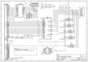
Schematic
Errata Version 1.0 of the schematic and PCB label resistors R1, R2, R3 and R4 as 100k, but it was found that if all four inputs were set to the RC2014 bus primary clock (CLK) the system would become unreliable. The value has therefore been changed to 470k to reduce loading of the clock signal.
5
What You Need The Z80 CTC module (SC102) is a very flexible board, with many options. It is therefore possible to assemble it in a variety of different configurations, such as not including the on-board oscillator. The following components are required to assemble the module with its full functionality and jumper options. Header pins JP1 to JP7, P1, P2 and P3 may need to be cut from longer strips. Image
Qty
1 4 1 5 7 1 1 1 4 1 1
Reference PCB
Description Printed circuit board SC102 Z80 CTC
C1, 2, 3, 4
Capacitor 100nF, ceramic, lead spacing = 2.54mm
JP1 and JP2
Pin header male 2x2 pins straight
JP3 - JP7
Pin header male 2x4 pins straight
JP1 - JP7 shunt
Jumper shunt for pin spacing = 2.54mm
P1
Pin header, male, angled, 2-row x 39-pin, 2 row (1 row optional)
P2
Pin header, male, angled, 1-row x 2-pin
P3
Pin header, male, angled, 1-row x 10-pin
R1, 2, 3, 4
Resistor 470k, axial, 5%, carbon film, 0.25W
RP1
Resistor pack 8x10k, SIL, 9-pin
SW1
DIP switch, 6 way, piano style
6
1 1 1 1 1 1
U1
74HCT688, 8-bit identity comparator, PDIP 20
U1 socket
20 pin PDIP IC socket 0.3" wide
U2
Z80 CTC, 8MHz, Z84C3008PEG (or Z80 CTC, 10MHz, Z84C3010PEG), PDIP 28
U2 socket
28 pin PDIP IC socket 0.6" wide
X1
Oscillator module 7.3728MHz, either 8 pin or 14 pin
X1 socket
14 pin PDIP IC socket 0.3" wide
Also required to assemble the module from the above components: Long nose pliers Side cutters Soldering iron Solder PCB cleaning materials
7
Components: What They Do & Where To Get Them Each component is described below. I have listed multiple sources for most components, but have not actually tried all of them, so best treat the specified part numbers as guidance only. Where eBay is listed as a supplier, the part is likely to be cheaper there than the other sources, sometimes considerably cheaper. Further savings are usually possible by ordering parts direct from countries like China.
PCB Image
Qty
1
Reference PCB
Description Printed circuit board SC102 Z80 CTC
Supplier EasyEDA
Part number Search EasyEDA.com for RC2014 CTC
The PCB is currently only available to be ordered from EasyEDA.com
C1, 2, 3, 4 Image
Qty
4
Reference C1, 2, 3, 4
Description Capacitor 100nF, ceramic, lead spacing = 2.54mm
Supplier Farnell Mouser RS
Part number 1100533 75-1C10Z5U104M050R 699-5027
These capacitors provide power supply decoupling (or bypass). The fast switching in digital circuits creates spikes on the power supply lines which are suppressed with decoupling capacitors placed at key points on the circuit board.
8
JP1 and JP2 Image
Qty
1
Reference JP1 and JP2
Description Pin header male 2x2 pins straight
Supplier eBay Farnell Mouser RS
Part number 200906546562 (2x40 pin to be cut to length) 2356151 (2x40 pin to be cut to length) 710-61308021121 (2x40 pin to be cut to length) 155-721 (2x40 pin to be cut to length)
This pair of jumpers allow the interrupt daisy chain signals to be connected to the RC2014 bus signal USER 2 (pin 38) and USER 3 (pin 39). To make use of this feature you must use a backplane that is specifically designed to provide the necessary daisy chain, such as Backplane SC107. The current official RC2014 backplanes do not support this feature. Alternatively the signals IEI and IEO can be found on connector P2 on the back edge of the board. Dupont wires can be used to daisy chain these signals to other modules.
JP3 - JP7 Image
Qty
5
Reference JP3 - JP7
Description Pin header male 2x4 pins straight
Supplier eBay Farnell Mouser RS
Part number 200906546562 (2x40 pin to be cut to length) 2356151 (2x40 pin to be cut to length) 710-61308021121 (2x40 pin to be cut to length) 155-721 (2x40 pin to be cut to length)
JP3 to JP6 allow the source for each CTC input to be set to any of: RC2014 bus primary clock (CLK) RC2014 bus secondary clock (CLK2) This module’s on-board oscillator clock signal (CLKX) RC2014 bus USER pin (USER 4, 5, 6, 1 for CTC inputs 0, 1, 2, 3) Without a jumper shunt fitted the input is from a pin on connector P3 on the back edge of the board.
9
JP7 allows the module to supply a clock signal to the RC2014 bus secondary clock (CLK2). The possible signal sources are: CTC channel 0 output (ZT0) CTC channel 1 output (ZT1) CTC channel 2 output (ZT2) This module’s on-board oscillator clock signal (CLKX)
JP1 - JP7 shunt Image
Qty
7
Reference JP1 - JP7 shunt
Description Jumper shunt for pin spacing = 2.54mm
Supplier eBay Farnell Mouser RS
Part number 201261690156 2396303 649-68786-102LF 674-2397
These shunts (small sockets) connect the required pins on JP1 to JP7. They may also be used to connect pins on P3, as described below.
P1 Image
Qty
1
Reference P1
Description Pin header, male, angled, 2-row x 39-pin, 2 row (1 row optional)
Supplier eBay Farnell Mouser RS
Part number 200906546562 (2x40 pin to be cut to length) 1097962 (2x40 pin to be cut to length) 571-9-103795-0 (2x40 pin to be cut to length) 155-743 (2x40 pin to be cut to length)
This connector mates with the RC2014 bus backplane. You can fit a single or a double row header, but the full functionality of this module requires the extended RC2014 bus and thus a double row header. Some pins need to be removed, using a pair of pliers, before fitting.
10
P2 Image
Qty
1
Reference P2
Description Pin header, male, angled, 1-row x 2-pin
Supplier eBay Farnell Mouser RS
Part number 200906546562 (1x40 pin to be cut to length) 2356192 (1x40 pin to be cut to length) 710-61304011021 (1x40 pin to be cut to length) 156-077 (1x40 pin to be cut to length)
As the official RC2014 backplanes do not provide a Z80 mode 2 interrupt daisy chain (IEI and IEO signals), these have been brought to the back of the board where they can be easily linked to other modules with Dupont wires.
P3 Image
Qty
1
Reference P3
Description Pin header, male, angled, 1-row x 10-pin
Supplier eBay Farnell Mouser RS
Part number 200906546562 (1x40 pin to be cut to length) 2356192 (1x40 pin to be cut to length) 710-61304011021 (1x40 pin to be cut to length) 156-077 (1x40 pin to be cut to length)
This connector brings power, oscillator output, CTC inputs and CTC outputs, to the back of the PCB. This makes it easy to connect via Dupont wires to other cards or to breadboards. This connector also allows a simple jumper shunt to connect the output of one CTC channel to the input of the next, thus allowing channels to be cascaded for greater range.
11
R1, 2 ,3 ,4 Image
Qty
4
Reference R1, 2, 3, 4
Description Resistor 470k, axial, 5%, carbon film, 0.25W
Supplier Farnell Mouser RS
Part number 9356819 652-4609X-1LF-10K 333-864
These resistors provide pull-ups for the CTC inputs so that they do not float up and down in the event a jumper is left off. Version 1.0 of the schematic and PCB label these as 100k, but it was found that if all four inputs were set to the RC2014 bus primary clock (CLK) the system would become unreliable. The value has therefore changed to 470k to reduce loading of the clock signal.
RP1 Image
Qty
1
Reference RP1
Description Resistor pack 8x10k, SIL, 9-pin
Supplier Farnell Mouser RS
Part number 9356819 652-4609X-1LF-10K 333-864
This is a network of 8 resistors with one end of each resistor common to pin 1. The resistors are used to pull up the address select switch (SW1) outputs and also to pull up the interrupt enable input signal (IEI).
12
SW1 Image
Qty
1
Reference SW1
Description DIP switch, 6 way, piano style
Supplier eBay Farnell Mouser RS
Part number 262361463572 2452331 653-A6FR-6104 (black) 877-2359
This switch is used to set the I/O address for the module. It sets the required state of address lines A2 to A7, thus allowing the module to occupy a 4 address block on any 4-byte boundary. In order to provide some certainty for software it is strongly recommended you set the base address of your first CTC module to 0x88, so that the module occupies I/O addresses 0x88 to 0x8B. This is done by setting switches 1 to 6, to Off, On, On, On, Off, On, where On is the switch closed. In the case of the piano style DIP switch, the On position is the switch lever pushed down towards the circuit board. Switches in the On position pull down the input of the address comparator U1. Switches in the Off position allow the input of the address comparator to be pulled up by RP1.
U1 Image
Qty
1
Reference U1
Description 74HCT688, 8-bit identity comparator, PDIP 20
Supplier Farnell Mouser RS
Part number 2407104 595-CD74HCT688E Surface mount HC only
This integrated circuit provides the address decoding, by comparing the current address from the CPU with the address set with the DIP switch SW1.
13
U1 socket Image
Qty
1
Reference U1 socket
Description 20 pin PDIP IC socket 0.3"
Supplier Farnell Mouser RS
Part number 4285608 571-1-2199298-6 674-2444
Reference U2
Description Z80 CTC, 8MHz, Z84C3008PEG (or Z80 CTC, 10MHz, Z84C3010PEG), PDIP 28
Supplier Farnell Mouser
Part number 6MHz version only 692-Z84C3008PEG (8 MHz version) 692-Z84C3010PEG (10 MHz version) 625-8996 (8 MHz version)
U2 Image
Qty
1
RS
The Z80 CTC provides a four channel programmable counter/timer. All four channels have an external clock/trigger input, and the first three channels have a zero count/time-out output. All of these signals are available on connector P3 on the back edge of the board. Each counter/timer channel can be started as a timer by an external trigger signal on the channel’s input. Each counter/timer channel can count down from a pre-set value, each time the selected edge (rising or falling) occurs on its input. When the counter reaches zero the counter is automatically reloaded and an optional interrupt generated. Feeding a clock signal to a CTC channel input enables the CTC to generate a periodic tick signal and/or interrupt. Jumper options allow each channel to be optionally supplied with a clock signal from one of these sources: RC2014 bus primary clock (CLK) RC2014 bus secondary clock (CLK2) The CTC’s on-board oscillator output (CLKX) RC2014 bus USER pin (USER 5, 6, 7, 1 for CTC channels 0 to 3) An external signal from connector P3 14
The first three channels can each act as a baud rate generator by generating a periodic output at the required frequency, as described above. By pre-setting a channel’s counter to 1 the CTC can generate a Z80 mode 2 interrupt each time the selected edge occurs on the channel’s input. This allows the CTC to act as a four channel Z80 mode 2 interrupt controller for non-Z80 devices. For further details see the Zilog CTC data sheet.
U2 socket Image
Qty
1
Reference U2 socket
Description 28 pin PDIP IC socket 0.6"
Supplier Farnell Mouser RS
Part number 2453476 571-1-2199299-2 674-2454
Reference X1
Description Oscillator module 7.3728MHz, either 8 pin or 14 pin
Supplier Farnell Mouser
Part number 2508742 (7.328MHz 8-pin QX8T50B) 774-MXO45HS-3C-7.3 (7.3728MHz 8-pin MXO45HS) 796-0574 (7.328MHz 8-pin QX8T50B)
X1 Image
Qty
1
RS
This oscillator is optional. If fitted it can perform a number of functions: Source for the RC2014 primary bus clock (CLK) Source for the RC2014 secondary bus clock (CLK2) Source for any or all of the CTC clock inputs The default assumption is that a 7.3728 MHz oscillator is used. By using this value the board will match the frequency expected by software designed for this board. It will also enable the oscillator to be useful as a source for the RC2014 bus clocks CLK and CLK2, which are usually 7.3728 MHz.
15
If this oscillator is not fitted, the board can be configured with jumpers to use either of the RC2014 bus clocks as a source for any or all of the CTC inputs.
X1 socket Image
Qty
1
Reference X1 socket
Description 14 pin PDIP IC socket 0.3"
Supplier Farnell Mouser RS
Part number 2445621 571-1-2199298-3 674-2438
16
Assembly Guide This guide assumes you are familiar with assembling circuit boards, soldering and cleaning. If not, it is recommended you read some of the guides on the internet before continuing. First check you have all the required components, as listed in the section “What You Need”. Header pins JP1 to JP7, P1, P2 and P3 may need to be cut from longer strips.
Step 1
Fit and solder the 4 resistors R1, R2, R3 and R4. Colour code for 470k resistor: Yellow, Violet, Yellow These can be fitted either way round, as they are not polarity dependent. These should be 470k resistors, not the 100k resistors shown on v1.0 schematic and circuit board.
17
Step 2
Fit and solder IC sockets for U1, U2 and X1.
Be sure to fit them with the notch matching the legend on the circuit board, so you do not end up fitting the IC the wrong way round too.
You may wish to solder the oscillator X1 directly to the board, in which case do not fit a socket in position X1.
18
Step 3
Fit and solder capacitors C1, C2, C3 and C4.
These can be fitted either way round, as they are not polarity dependent.
19
Step 4
Fit and solder resistor pack RP1.
This must be fitted the correct way round. The component should have pin 1 marked with a dot, as illustrated right.
20
Step 5
Fit and solder connector P1.
You can fit just a single row header as used by the RC2014 standard bus, but doing so means not all the features of this module can be used. It is best to fit a double row even if the module is initially only used with a standard bus backplane. To prepare the header, it should first be cut to length (if starting with a strip more than 39 pins long) and then unwanted pins must be removed. If you want to make the board as easy to insert and remove as possible, you can remove all the pins in the second row except those shown on the schematic as used and indicated below in green. Take care to ensure the pins are parallel to the circuit board so that the board will be vertical when plugged into a backplane.
21
Step 6
Fit and solder connector P2 and P3.
Take care to ensure the pins are parallel to the circuit board.
22
Step 7
Fit and solder header pins JP1 to JP7.
JP1 and JP2 are made up of a single header 2 pins by 2 pins as illustrated right.
23
Step 8
Fit and solder the DIP switch SW1.
In order to provide some certainty for software it is strongly recommended you set the base address of your first CTC module to 0x88, so that the module occupies I/O addresses 0x88 to 0x8B. This is done by setting the switches as illustrated below.
If you have a second CTC module the recommended base address is 0x8C.
24
Step 9 Remove any solder ‘splats’ with a brush, such as an old toothbrush. Visually inspect the soldering for dry joints and shorts. Clean the flux off with suitable cleaning materials. Visually inspect again. Before fitting the ICs, plug the board into an RC2014 backplane with no other boards fitted. Power the backplane and perform the following checks with a volt meter: Check the supply voltage on the CTC module, between, say, U1 pin 10 and U1 pin 20. This should be 4.5 to 5.5 volts, preferably 4.75 to 5.25 volts. Check each input (CT0, CT1, CT2 and CT3) on connector P3 is being pulled up to at least 4.5 volts. Check the interrupt enable input (IEI) on connector P2 is being pulled up to at least 4.5 volts. Check each address switch input (Q2 to Q7) on U1 is being pulled up to at least 4.5 volts when the appropriate switch (SW1) is Off (open) and drops to less than 0.4 volts when the appropriate switch (SW1) is On (closed). If you have an oscilloscope or logic probe, check the clocks CLK, CLK2 and CLKX at jumper header JP6. If all is well, power down and remove the CTC module.
25
Step 10 Insert the ICs into their sockets, taking care to insert them the right way round, as illustrated below. Be careful not to bend any legs over.
There is no need to fit any of the jumper shunts yet. Now plug the CTC module into the RC2014 backplane together with your normal working set of modules. Power up and check the system is working as usual.
26
Configuring the CTC Module The following are just a few examples of how you can configure and use the CTC module. To realise its full potential it is necessary to study the Zilog Z80 CTC data sheet, which can be found on the internet by searching for “zilog UM0081”. Most of the following examples require software support.
CTC Module as the Primary Clock The CTC module can provide a clock source for the RC2014 bus primary clock (CLK). This means a separate clock module is not required, potentially saving one backplane slot. The illustration below shows the jumper shunt positions required to link the output of the on-board oscillator to the RC2014 bus primary clock (CLK). The illustration uses JP4, but any of the jumpers JP3 to JP6 can be used.
27
Input Each channel’s counter/timer input can be either: RC2014 bus primary clock (CLK) RC2014 bus secondary clock (CLK2) The CTC’s on-board oscillator output (CLKX) RC2014 bus USER pin (USER 5, 6, 7, 1 for CTC channels 0 to 3) An external signal from connector P3 The illustration below shows the jumper shunt positions for: Channel 0 to use the RC2014 bus primary clock (CLK) as its input Channel 1 to use the RC2014 bus secondary clock (CLK2) as its input Channel 2 to use the on-board oscillator clock (CLKX) as its input Channel 3 to use the signal on RC2014 bus pin 37 (USER1) as its input To use the signal on P3’s CT0, CT1, CT2 or CT3 input, just remove the channel’s input jumper shunt so the input is not connected to any of the above.
This feature requires software support.
28
Output The outputs from channels 0 to 2 (ZT0, ZT1 and ZT2) are connected to P3, so that they can be easily accessed for any required purpose. Channel 3 does not have an accessible output signal. In addition, the outputs are connected to jumper JP7, along with the on-board oscillator clock (CLKX). Jumper JP7 enables the RC2014 bus secondary clock (CLK2) to be supplied by any one of the CTC outputs or the on-board oscillator output (CLKX). By using a CTC output as the secondary clock source, port B of the serial SIO module can have its baud rate controlled by software. If your RC2014 system already has a device providing the secondary clock signal (CLK2), then do not fit a jumper shunt to JP7. The illustration below shows the jumper shunt position required to use the output of CTC channel 1 as the source for the secondary bus clock (CLK2).
This feature requires software support.
29
Baud Rate Generator For users of the official RC2014 Z80 SIO/2 module, the CTC module can provide a software selectable baud rate clock for SIO port B. In the example below, the normal clock module is removed and the CTC module provides the RC2014 bus primary and secondary clocks (CLK and CLK2). The primary clock (CLK) is 7.3827 MHz, while the secondary clock (CLK2) is 0.6144 MHz. The primary clock is used by the processor and by SIO port A (115200 baud), while the secondary clock is used by SIO port B (9600 baud).
The jumper shunt positions shown above perform the following functions: Red Sets the RC2014 bus primary clock (CLK) to the CTC module’s on-board oscillator output (CLKX). Green Sets CTC channel 1 clock input to the CTC module’s on-board oscillator output (CLKX). Yellow Links CTC channel 1 output to the RC2014 bus secondary clock line, providing the baud rate clock for SIO port B. The SIO/2 module’s port B jumper shunt should be removed to isolate port B’s clock from port A’s clock. To set CTC channel 1 to generate the required 0.6144 MHz clock, issue the following Small Computer Monitor commands: O 89 55 O 89 6 30
Or the BASIC commands: OUT &H89, &H55 OUT &H89, 6 Where: &H89 is the address of CTC channel 1’s control register (&H88+1) &H55 selects: No interrupt Counter mode Count on rising edge Time constant follows 6 is the time constant The time constant value 6 selects divide by 12. The doubling of the divider, or halving of the frequency, is caused by the CTC only counting the second edge. With the CTC input at 7.3728 MHz and CTC channel 1 set to divide by 12, CTC channel 1 output is 7.3728 / 12 MHz, which is 0.6144 MHz. The 0.6144 MHz clock is output to the RC2014 secondary clock line (CLK2) and is picked up by SIO/2 port B. By default the SIO is set to divide the incoming clock by 64 to generate the baud rate. The baud rate is thus 0.6144 / 64 MHz, which is 0.0096 MHz or 9600 Hz. Time constant value and baud rates: SIO divider = 16 Constant Baud rate 1 230400 2 115200 4 57600 6 38400 12 19200 16 14400 24 9600 48 4800 96 2400 192 1200
SIO divider = 64 (default) Constant Baud rate 1 57600 2 28800 3 19200 4 14400 6 9600 12 4800 24 2400 48 1200 96 600 192 300
31
Cascading Channels By linking the output of one CTC channel to the input of the next, the two channels can be cascaded to give a greater range. The illustration below shows the jumper shunt position required to link the output of channel 1 to the input of channel 2.
This feature requires software support.
32
Interrupt Controller The CTC module can act as an interrupt controller, whereby it provides Z80 interrupt mode 2 functions for up to four devices that do not themselves support mode 2. The illustration below shows the jumper shunt positions (in red) required to use channel 1 and channel 3 as interrupt controllers for non-mode 2 devices. The interrupt signals from the non-mode 2 devices can be connected to CT1 and CT3 on P3 (shown in yellow) with Dupont wires, or to USER pins on the RC2014 bus (shown in green).
This feature requires software support. The software will be required to: Set the processor to interrupt mode 2 and initialise the I register Set the interrupt vector table entries for the CTC’s interrupts Set the CTC’s interrupt vector register Set the CTC channel(s) to count down from 1 Set the CTC channel(s) input edge to either rising or falling Set the CTC channel(s) to generate an interrupt Write an interrupt handler for the non-mode 2 device
33
Interrupt Daisy Chain If your system has more than one device using interrupt mode 2, it will be necessary to set up an interrupt daisy chain. This is fully described in the Z80 peripherals data sheet, but essentially it requires linking the output (IEO) of one interrupt generating device to the input (IEI) of the next, and so on. The position in the chain determines the device’s interrupt priority. The illustration shows the connections required when using external Dupont wires on P2 (in red) and the RC2014 bus USER pins (in yellow).
This feature requires software support. Setting up a mode 2 interrupt system is not trivial so requires study of the data sheets rather than following any simple example I could write here.
34
Fault Finding Check all links and jumpers, check no chips have bent legs and thus not making contact with their socket, carefully inspect all soldering, check all the chips are inserted the right way round, check all the components are in the right place. With the CTC module plugged in to the RC2014 backplane with no other boards fitted. Power the backplane and perform the following checks with a volt meter: Check the supply voltage on the CTC module, between, say, U1 pin 10 and U1 pin 20. This should be 4.5 to 5.5 volts, preferably 4.75 to 5.25 volts. Check each input (CT0, CT1, CT2 and CT3) on connector P3 is being pulled up to at least 4.5 volts. Check the interrupt enable input (IEI) on connector P2 is being pulled up to at least 4.5 volts. Check each address switch input (Q2 to Q7) on U1 is being pulled up to at least 4.5 volts when the appropriate switch (SW1) is Off (open) and drops to less than 0.4 volts when the appropriate switch (SW1) is On (closed). If you have an oscilloscope or logic probe, check the clocks CLK, CLK2 and CLKX at jumper header JP6.
35
History 2018-06-05 2018-06-22
v1.0 v1.1
First circuit boards R1,2,3,4 changed from 100k to 470k due to loading of bus clock causing unreliability of system Schematic and PCB silk screen changed to show 470k
36
Contact Information If you wish to contact me regarding this document, or the hardware and software it relates to, use the contact page at www.scc.me.uk Stephen C Cousins, Chelmsford, Essex, United Kingdom.
RC2014 information Information about the RC2014 system can be found at www.rc2014.co.uk
RC2014 support Issues related to the RC2014 can be posted on the google group “RC2014-Z80”.
RC2014 supplies Parts can be purchased through Tindie at www.tindie.com (search “RC2014”) Official RC2014 parts are at: https://www.tindie.com/stores/Semachthemonkey/?ref=offsite_badges&utm_sour ce=sellers_Semachthemonkey&utm_medium=badges&utm_campaign=badge_medi um
Credits Thanks to all those who provided encouragement, feedback and contributed ideas to the design. Specifically: Mark T, Tom S, Jon L, Nigel K, Samster, Jay C, Colin L, Karl B, Spencer O, and anyone else I forgot! See RC2014 google group for full details: https://groups.google.com/forum/#!topic/rc2014-z80/4s1pwSQoddQ
37