Effect of access resistance on apparent mobility reduction in nano-MOSFET K. Huet, J. Saint-Martin, A. Bournel, D. Querlioz, P. Dollfus IEF, Univ. Paris Sud, CNRS, Orsay 91405, France
[email protected]
Abstract —Thanks to both device simulation and ballistic calculation, the concept of apparent mobility is discussed in the case of unstrained and strained nanoscale DG MOSFET. We show that the apparent mobility reduction in simulated short channel devices can be explained by non stationary effects. The apparent mobility is successfully linked to the long-channel mobility and to a "ballistic mobility" using a Mathiessen's rule. Moreover, a simple extended expression of the ballistic mobility in the Shur analytical model suggests the non-universal nature of this parameter through its dependence on drain voltage, access resistance and device geometry. The effect of access resistance is analyzed in more details by means of ballistic calculations. The results are consistent with that obtained from both Monte Carlo simulation and measurements.
I.
II.
EXTRACTION METHOD
In this paper, the apparent mobility µextr was extracted from drain current ID variations as a function of the gate voltage VGS at low drain voltage VDS using a method inspired by Hamer [14]. The following formula was used to fit the I-V characteristics:
I Hamer = CGS D
µeff W VDS , ( VGS − VT ) Lch 1 + θ ( VGS − VT )
(1)
where the gate capacitance CGS is given by the analysis of charge vs. gate voltage curves [15]. The threshold voltage VT, the extracted effective mobility µeff and the gate field reduction parameter θ which includes the access resistance effect were used as fitting parameters.
INTRODUCTION
The mobility is widely used in microelectronics as a measurable factor of merit of a technology and it is still the key parameter in most analytical models to predict device performance. However, an unexpected apparent reduction of the mobility at short gate length has been experimentally observed by many groups [15]. The interpretation of such a behavior is giving rise to a growing debate. In particular, doping pockets and charge or neutral defects are suspected of limiting the mobility when MOSFETs are scaled down. However, the assumption that the measured mobility in nanoscale devices is actually the “classical” mobility of the channel can be questioned [6, 7]. Indeed this concept results from an analysis of stationary transport where scattering phenomena limit the carrier velocity. If scattering cannot be neglected [8-10] in decananometer MOSFET, ballistic transport in the channel takes a growing importance as the gate length of MOSFETs tends to the nanometer scale. Besides, analytical and compact models [11-13] suggest that the observed mobility reduction could be only apparent and mainly the consequence of non stationary effects. After presenting the mobility extraction method used in this paper, the influence of the access resistance on apparent mobility in ballistic channel is investigated analytically and numerically. At last, a “Matthiessenlike” model involving the ballistic mobility is tested to fit simulated and experimental results.
III.
MODELLING OF APPARENT AND BALLISTIC MOBILITY
According to Shur's approach suggested in [12], the apparent or effective mobility µeff in a standard device may be given by the "Mathiessen-like" expression
µeff =
(2)
1 −1 −1 µlong + µbal
where µlong is the long channel mobility and µbal is the “ballistic mobility” assumed to be Lch dependent (3)
µbal = K bal .L ch
To express the apparent mobility in ballistic channels, we used a ballistic model where access resistances are included as follows [16]
I
bal D
= WCGS ( V GS − VT ) v th '
′ = VGS − R I (VGS′ , VDS′ ) , VGS ′ = VDS VDS
UT
'
UT
1 + e − V DS
bal S D
− (R S + R D )I (VGS′ , VDS′ ) , bal D
'
1 − e− V DS
(4) (5) (6)
where U T = k B .T q , W is the channel width, CGS is the gate capacitance, VT is the threshold voltage, RS (RD) is the source (drain) access resistance, q is the electron charge, vth the average thermal velocity, kB the Boltzmann constant and T the temperature. VDS and VDS’ (VGS and VGS’) are the extern and intrinsic drain
I
bal D
CGS .v th .W ( VGS − VT ) × sinh ( VDS U T )
=
1 + cosh ( VDS
R S .sinh ( VDS U T ) U T ) + W.CGS .v th + ( R S + R D ) × V −V / U ( ) T T GS
Identifying this expression with the Hamer expression (1) commonly used to extract access resistances, i.e. θ = W. Keffbal.Cox.(Rs.+Rs), gives K bal eff =
v th sinh ( VDS U T )
are taken into account by interpolating the current using equations (5) and (6).
Drain current ID (µA/µm)
(gate) bias, respectively. Using the first order terms of the Taylor expansion gives
600 vinjbal (107cm.s-1) 1,2
500
2Dk Fermi
400
Inversion density NS
300
100
(7)
0.1
ID = q ∑ bal
∑ ∫
valleys subbands
v + D + (E)f (ϕFS , E) (1 − f (ϕFD , E) )
− v − D − (E)f (ϕFD , E)(1 − f (ϕFS , E)) dE Where D+/-(E) is the Density Of State (DOS) at a given energy E in the source and drain, respectively, φFS (φFD) is the Source (Drain) and f is the Fermi-Dirac occupation function. The injection velocity v+ used in Eq. (1) is presented in the inset of Figure 1 as a function of the inversion charge. The access resistances
0.3
0.4
0.5
0.6
0.7
0.8
Figure 1: ID-VGS characteristics for ballistic channel devices obtained with Natori model[16, 17] and Schred[18], including Rs influence. RS = 0 (open squares), 25 (open circles), 50 (open triangles), 100 (close squares), 150 (close circles), 200 (close triangles), 300 (close diamonds) and 450 Ω.µm (close diamonds) . Dashed line, ballistic channel MC 3Dk characteristic. Inset: Injection velocity according to the electron density for Boltzmann and Fermi statistics.
16
0.5
14
DG
0.4
12 10
0.3
8
SG
6
0.2
4
0.1
2 0
This analytical model only provides a rough approximation at low VDS and RS and takes into account neither complex electrostatic gate control nor quantization effects. For completing this lacks, we used a multi subband 2DEG ballistic formalism as developed in [16, 17]. The inversion density and the electrostatic potential in the transverse direction were obtained by solving the 1D Schrödinger and Poisson equations self consistently[18], considering FermiDirac statistics. The current was then calculated with the Landauer formula for a degenerate electron gas [17], considering a transmission coefficient equal to 1 i.e.
0.2
Gate Voltage VGS(V)
0
100
200
300
400
1/Kbal (cm-2.V1.s1.nm1)
This expression of Kbaleff, though over-simplified, is meaningful. The theoretical maximum value of Kbal obtained for VDS = 0 and RS = 0 is equal to 20 cm2V-1s-1. This result is similar to Shur calculation [12] by using the convenient thermal velocity. More interesting, Eq. (7) suggests that Kbal depends on the extrinsic parameters CGS, RS and VDS. Therefore, the extracted apparent mobility seems to unfortunately depend on the source access resistances in ballistic channel.
Rs (Ω.µm)
0 0
Kbal (cm2.V-1.s-1.nm-1)
2.U T VDS2 1 = + CGS .R S .W.VDS + + O(VDS3 ) bal K eff v th 6.v th U T
1013
DG-MOS, TSi = 5 nm, VDS = 50 mV
CGS v th W R S VDS - (R S + R D ) ( VGS − VT ) sinh ( VDS U T )
should be extracted at VGS providing the maximum transconductance i.e. at VGS close to VT. Finally, neglecting higher order VDS terms leads to
1
(cm-2)
1012
200
VDS 1+cosh ( VDS U T ) + CGS v th W (R S + R D ) ( VGS − VT ) U T +
Keffbal
MC 3Dk
3Dk Boltzmann
0
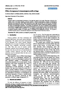
Access resistance RS (W.µm) Figure 2: Keffbal (RS) extracted from 2DEG Landauer formalism, VDS = 50 mV for various unstrained device geometries. Open symbols: DG structures (CGS = 0.047 F/m2). Close symbols: SG structures (CGS = 0.022 F/m2). TSi = 5 nm (squares), 9 nm (triangles), 15 (circles).
The resulting electrical characteristics of a 5 nm thick DGMOSFET with an equivalent oxide thickness (EOT) of 1.1 nm at VDS = 50 mV are reported on Figure 1 for different RS values. A rigid VGS shift has been applied in order to account for the confinementinduced threshold voltage shift. The ID(VGS) characteristic obtained for RS = 25 Ω.µm is very close to the MC simulation result for the ballistic channel devices (dashed line). The extracted Kbal by the Hamer method is plotted in Figure 2 as a function of Rs. Results for SG and different TSI are also presented. This evolution qualitatively follows Eq. (7). Indeed the origin of all curves is nearly equal to 15 cm2.V-1.s-1.nm-1 as expected for VDS = 50 mV. Moreover the behavior of 1/Kbal(Rs) for the studied structures is nearly linear with RS and the slopes are
mainly governed by the gate capacitance which is quasi proportional to the number of gates. In the studied SG-MOSFET, Kbal varies from 16 to 3 cm2.V-1.s-1.nm-1 when RS varies from 0 to 500 Ω.µm. Kbal is also sensitive to CGS which is influenced by the geometry. The difference between SG and DG is almost constant in the range of studied RS and equal to 2 cm2.V-1.s-1.nm-1. As a conclusion, in the used extraction method the gate capacitance and the access resistance certainly have a significant impact on the extracted ballistic apparent mobility if the drain voltage is not very small.
IV.
MONTE CARLO RESULTS
Mobility (cm2.V-1.s-1)
The channel length Lch of the studied DG structures ranged from 10 nm to 400 nm. The body thickness TSi was equal to 5 nm and the gate oxide thickness Tox (or equivalent oxide thickness, EOT) was 1.2 nm. Two series of devices were simulated: DG MOSFETs in which standard scattering rates have been considered in the channel and artificial structures with the same geometry but with ballistic channels, i.e. without any scattering events. The channels were non intentionally doped, thus favoring ballistic transport. The temperature is T = 300 K, unless otherwise stated. We consider a metallic midgap gate material. Strained devices have also been investigated. ION (µA.µm-1)
1600
In all studied devices (ballistic or not), the extracted VT (not shown) is found almost constant (within the 0.289 – 0.295 V range), except for the 10 nm device which suffers from SCE (VT = 0.269 V). VT variations are therefore clearly not responsible for the ID enhancement at short Lch. The extracted mobility for diffusive channel is shown in Figure 3 (symbols). The decreasing behavior of µeff with Lch is similar to experimental observations although the interaction mechanisms considered in our simulations are identical for all Lch. Consequently, this apparent mobility reduction is not related to any additional scattering phenomena specific to short channel devices, as suggested elsewhere [19]. Table 1: Model parameters deduced from MC simulations
Simulated µlonga Kbalb vsat c (cm2.V-1.s-1) (cm2.V-1.s-1.nm-1) (×107cm/s) devices Unstrained, 510 8.4 1.0 T = 300 K Unstrained, 355 7.2 1.0 T = 400 K Strained, 1000 13.2 1.2 T = 300 K a b from 5 nm-thick long-channel devices MC, from ballistic channel devices MC c from bulk material in a constant field MC.
1500 1000
1200
500 0
µeff/Lch (cm2.V-1.s-1.nm-1) 1
2
3
4
5
800 400 0 0
scattering was considered for short channel length devices. An analytical description of the conduction band structure is used with 6 non-parabolic ellipsoidal ∆ valleys (see for example [9] and references therein for more details on MONACO).
100
200
300
400
Channel Length Lch (nm) Figure 3: Mobility extracted from Monte Carlo simulation ID(VGS) curves at low VDS as a function Lch (symbols). Circle: Unstrained silicon 400 K. Square. Unstrained silicon 300 K. Strained silicon 300 K. Continuous line: “Matthiessen-like” model. Dashed line: linear fits for strainded ballistic channels 300 K. Inset: Correlation between ON current (obtained in the saturation regime, VDS=VGS=0.7 V) and effective mobility (obtained in the linear regime).
The studied devices have been simulated by using our semi-classical particle Monte Carlo device simulator MONACO coupled with a 2D Poisson solver. In this work, scattering mechanisms related to phonons, ionized impurities and SiO2/Si surface roughness (via an empirical combination of diffusive and specular reflections) are included. No additional
The interest of using this apparent mobility as a factor of merit is illustrated in the inset of Figure 3. Indeed, this parameter evaluated at low drain voltage appears to be strongly correlated to the on-state current, for all studied devices, even if the dominant scattering mechanisms can differ between the linear and the saturation regimes. Pragmatically, the apparent mobility could be used relevantly in macroscopic analytical models. In ballistic channels the apparent mobility (shown in Figure 3 for strained Si channel) varies linearly with the channel length as predicted by Shur in eq. (3). The corresponding Kbal deduced from Monte Carlo ballistic channel simulation are reported in Table 1. In this table, µlong was obtained from long device simulations. For the device geometry used in MC simulation (TSi = 5 nm, RS = 38 Ω.µm), Keffbal extracted from the 2DEG calculation is equal to 8.2 cm2.V-1.s-1.nm-1(cf. Figure 2). It is in excellent agreement with the value extracted from a linear fit of the µeffbal(Lch) characteristic obtained by MC simulated devices. This shows that although the carrier degeneracy induces a significant difference in injection velocity (Figure 2), it does not change the value of the apparent mobility. A very good analytical approximation of µeff(Lch) is obtained and plotted on Figure 3 (continuous lines) by
introducing in a “Matthiessen-like” model (cf. Eqs. (2) and (3)) the Kbal values extracted from ballistic MC simulations and µlong of Table 1 for all simulated devices. This close agreement implies that the mobility degradation at reduced Lch can be mostly explained in this case by non stationary transport. Nevertheless, the accurate determination of Kbal(RS,CGS) requires the used of numerical simulation of ballistic channel.
with only one new parameter, the apparent ballistic mobility which depends linearly on the channel length. However, determining this parameter is not an easy task. Indeed the apparent ballistic mobility is related to the applied drain voltage and common extraction methods seem to fail to dissociate the influence of this parameter from that of access resistances and gate capacitances. ACKNOWLEDGMENTS:
V.
EXPERIMENTAL COMPARISON
This “Matthiessen-like” model (cf. eq. (2) and (3)) has been used to fit experimental results available in the literature. As shown in Figure 4, data from unstrained FD-SOI MOSFET [5] and DG MOSFET [20] was well reproduced knowing µlong and using Kbal as a fitting parameter. The extracted value of Kbal: 8.4 cm2.V-1.s-1.nm-1 and 3.6 cm2.V-1.s-1.nm-1 are in the range of values obtained in Figure 2 for ballistic device with access resistances and capacitance in the same order of magnitude.
Mobility µeff (cm2.V-1.s-1)
These results suggest again that the mobility degradation with reducing Lch could be explained by non stationary transport since the influence of access resistance and gate capacitance is well controlled.
This work was supported by the European Community, through Integrated Project PULLNANO (IST-026828) and Network of Excellence NANOSIL (ICT-216171), and by the French National Agency (ANR), through project MODERN (ANR-05-NANO002).
REFERENCES [1] [2] [3] [4]
1000 [5] [6]
constant µeff
[7] Kbal = 8.4
100
Kbal = 3.6
[8]
Symbols: exp. Lines: µeff(L) model
10
100
1000
Effective Channel Length Leff (nm) Figure 4: Experimental mobility [5] (triangles) [20] (circles). Continuous line: “Mathiessen-like” formalism using Kbal = 8.4 cm2.V-1.s-1.nm-1 and 3.6 cm2.V-1.s-1 nm-1. Dashed line: standard long channel mobility.
[9] [10] [11] [12] [13] [14]
VI.
CONCLUSION
In short channel, the apparent mobility extracted from ID(VGS) curves is not a real mobility in the stationary definition of the term. However, this apparent mobility can still be used to evaluate the ON state current of the transistor within a compact model. For the simulated devices with no new scattering phenomena, the extracted apparent mobility behavior with shrinking channel length was similar to that of experimental measurements. The mobility degradation in short channel, mostly explain by ballistic effects, can be well reproduced by a Shur “Matthiessen-like” model
[15] [16] [17]
[18] [19] [20]
K. Romanjek, F. Andrieu, T. Ernst et al., Solid-State Electron. 49, 721 (2005). J. Lusakowski, W. Knap, Y. Meziani et al., Appl. Phys. Lett. 87, 053507 (2005). W. Chaisantikulwat, M. Mouis, G. Ghibaudo et al., Solid-State Electron. 50, 637 (2006). J. Widiez, T. Poiroux, M. Vinet et al., IEEE Trans. Nanotechnology 5, 643 (2006). A. Cros, K. Romanjek, D. Fleury et al., IEDM (2006). K. Huet, J. Saint-Martin, A. Bournel et al., in Proc. ESSDERC, pp. 382 (2007). C. Jungemann, T. Grasser, B. Neinhuus et al., IEEE Transactions on Electron Devices 52, 2404 (2005). A. Svizhenko, and M. P. Anantram, IEEE Trans. Electron Devices 50, 1459 (2003). J. Saint Martin, A. Bournel, and P. Dollfus, IEEE Trans. Electron Devices 51, 1148 (2004). P. Palestri, D. Esseni, S. Eminente et al., IEEE Trans. Electron Devices 52, 2727 (2005). G. Baccarani, and S. Reggiani, IEEE Trans. Electron Devices 46, 1656 (1999). M. S. Shur, IEEE Electron Device Lett. 23, 511 (2002). J. Wang, and M. Lundstrom, IEEE Trans. Electron Devices 50, 1604 (2003). M. F. Hamer, IEE proceedings. Part I. Solid-state and electron devices 133, 49 (1986). J. Saint-Martin, A. Bournel, and P. Dollfus, Solid-State Electron. 50, 94 (2006). M. Lundstrom, and J. H. Rhew, Journal of Computational Electronics 1, 481 (2002). K. Natori, T. Shimizu, and T. Ikenobe, Japanese Journal of Applied Physics Part 1-Regular Papers Short Notes & Review Papers 42, 2063 (2003). D. Vasileska, S. S. Ahmed, M. Mannino et al., in Schred (2006). C. Dupré, T. Ernst, J. M. Hartmann et al., Journal of Applied Physics 102, 104505 (2007). F. Andrieu, in CEA-LETI (2005).