© 2008 OSA / FiO/LS/META/OF&T 2008
MMA2.pdf MMA2.pdf
Experimental Demonstration of Optical Nanofocusing by a Plasmonic Dimple Lens Hyojune Lee1, Shantha Vedantam1, Japeck Tang1, Josh Conway1,2, Matteo Staffaroni1, and Eli Yablonovitch1,3 1 Electrical Engineering Department, University of California, Los Angeles, California 90095 2 The Aerospace Corporation, El Segundo, California 90245 3 Department of Electrical Engineering & Computer Sciences, University of California, Berkeley, California 94720 Contact author:
[email protected]
Abstract: This paper reports the first experimental characterization of Plasmonic Dimple Lens structure that can focus optically-coupled surface plasmons to a nanoscopic volume beyond the diffraction limit, using the near-field scanning optical microscopy (NSOM) technique. © 2008 Optical Society of America OCIS codes: (240.6680) Surface plasmons
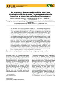
1. Introduction Focusing electromagnetic energy to sub-wavelength dimensions has become an increasingly active field of research for a variety of applications such as Heat Assisted Magnetic Recording (HAMR)[1], nanolithography[2], and nanoscale optical characterization of biological cells and single molecules using near-field scanning optical microscopy (NSOM) technique[3]. Conventional optics can only focus light to a diffraction-limited spot size of approximately λ/2n in a medium with refractive index n. Confining light through metal-clad fibers with subwavelength core size, field enhancement at the apex of sharp tips [4,5], are some of the common ways to get nanoscale focusing on the order of less of 100 nm. However the power efficiency in these approaches is very low [6,7]. Optical free space photons can be efficiently coupled to the nanoscale via surface plasmons. Surface plasmons are electronic excitations of free electron gas of a metal at a metal-dielectric interface, oscillating at optical frequencies. Photons coupled via plasmons can be focused to a smaller spot size, thus beating the diffraction limit on optical focusing [8]. This paper briefly describes an optimal design [9], a fabrication strategy [10] and the first experimental characterization of a novel plasmonic lens to focus surface plasmons. 2. Theoretical Background It has been shown [9,11] that double-sided surface plasmons can confine light to the nanometer scale by decreasing the insulator thickness of the metal-insulator-metal stack. Fig.1a shows the dispersion relation of a Au-SiO2-Au stack for various dielectric thicknesses using the optical constants of gold [12]. It is evident from the graph (Fig.1a) that for a fixed wavelength of operation, say 633 nm (1.96 eV), the double-sided surface plasmon wavelength can be varied from 390 nm to less than 20 nm by varying the thickness of SiO2 from 100 nm down to 1 nm. This graph forms the basis of our novel focusing structure which we call a plasmonic dimple lens (Fig.1b). Plasmon wavelength (in nm) 200 100
50 40
30
d = 20nm
2.5
15
20
10
d = 5nm d = 2nm
far-field from conventional lens
Photon energy (in eV)
d = 1nm
2.0
dimple lens
1.5
Au 1.0
SiO2
metal insulator metal
d
Au 0.5
0
0
0.1
0.2
0.4
0.3
0.5
0.6
Plasmon wave-vector ( 2π / wavelength(in nm))
(a)
0.7
in-coupling grating
focal spot
(b)
Fig.1 (a) Calculated dispersion relations for the Au-SiO2-Au stack for various thicknesses of the SiO2 layer (b) Perspective view of the plasmonic dimple lens
© 2008 OSA / FiO/LS/META/OF&T 2008
MMA2.pdf MMA2.pdf
The three-dimensional plasmonic dimple lens focuses double-sided surface plasmons in the plane normal to the layers of the stack. An optimal taper angle ensures efficient coupling of electromagnetic energy from larger plasmonic wavelengths to nanoscale plasmonic wavelengths with minimum resistive and reflective energy losses [9]. A circular grating coupler is designed to couple free space visible light into single-sided surface plasmons before they traverse the taper to the out-coupling facet. The plasmons assume shorter wavelengths as they propagate across the taper. The design parameters and field enhancement estimates can be found in ref. 9. The short plasmonic wavelengths at the end of the taper give rise to evanescent energy density at the focal spot on the out-coupling facet. Thus, optical focusing is achieved in all three dimensions that confines energy to nanoscopic volume. 3. Fabrication and Measurement The critical dimension determining the spot size of the focused plasmonic energy structure shown in Figure 1b is the final thickness of the dielectric at the end of the taper. The challenges faced in order to realize a three dimensional circular dimple in a dielectric, achieving a smooth and thin critical layer of dielectric, and issues of delamination between several layers faced during the mechanical-polishing of layers of dissimilar materials, are discussed in reference [10]. The overall fabrication strategy and sequence is discussed elsewhere [10]. Figure 2a depicts the outcoupling facet of the structure that was used in the experimental characterization. PMT pulled fiber NSOM probe
plasmonic dimple lens
Laser x-y-z control feedback
(a)
Stage
(b)
Fig.2 (a) Phase-shift AFM image of the out-coupling edge after mechanical edge-polishing. The size of the scan is 1.5 µm x 1.5 µm.. (b) Schematic of the experimental setup to characterize the plasmonic dimple lens facet (a) with a metal-clad pulled fiber probe employed in Nearfield Scanning Optical Microscopy (NSOM) technique.
The fabricated structure (Figure 2a) was characterized using a modified Veeco Aurora-3 NSOM system which uses shear-force feedback for scanning. A schematic of the measurement setup is shown in Figure 2b. The sample was mounted vertically on the NSOM stage so that the polished out-coupling edge of the device points upwards. 633 nm light from a HeNe laser was focused from the side onto the grating region of the device using a microscope objective (50X, 0.45 NA). The out-coupled light from the device was collected with a photo-multiplier tube (PMT) through a commercially available pulled-fiber NSOM probe. The sample was scanned with the NSOM tip to acquire both the topographic and the optical data at the same time. Figures 3a,b show good correlation between the region of high intensity of light in the optical image with the dimple region of the device in the topographic scan. Furthermore the spot size formed by the dimple lens is smaller than that formed by the circular grating coupler alone, as evident from Figure 3b and 3d respectively. It is important to note that the absolute spot size measurement in Figures 3b,d is believed to be limited by the size of the pulledfiber probe aperture (which varies between 100-150 nm) used in NSOM measurement system. 4. Conclusions In conclusion, we have designed, fabricated and characterized a novel plasmonic dimple lens structure in Audielectric-Au geometry for focusing visible light to the nanoscale. Comparison of measurements of the circular grating coupler alone and the circular grating coupler together with a dimple lens reveal additional focusing provided by the plasmonic dimple lens. However, the absolute measurement of the spot size produced by the dimple lens was not possible due to the aperture size limitation of the pulled-fiber NSOM probe used in the experiment. Our plasmonic lens is capable of focusing light to spot sizes smaller than the aperture size of the commercially available pulled-fiber NSOM probes. To overcome this problem, efforts are on to use a sharp dielectric tip to scatter the light
© 2008 OSA / FiO/LS/META/OF&T 2008
MMA2.pdf MMA2.pdf
from out-coupling facet. This approach will be limited by the radius of curvature of the dielectric tip which can be as small as 10-15nm [13].
Figure 3 (a) Topographic and (b) optical images of the out-coupling facet of the plasmonic dimple lens obtained by NSOM technique. (c) Topographic and (d) optical images of the polishing facet of the circular grating coupler only (without a plasmonic dimple lens). All the scans are 2.5 µm x 2.5 µm.
5. References [1] William A. Challener, Terry W. Mcdaniel, Christophe D. Mihalcea, Keith R. Mountfield, Kalman Pelhos and Ibrahim K. Sendur, “Light Delivery Techniques for Heat-Assisted Magnetic Recording,” Jpn. J. Appl. Phys. 42, p981-988 (2003) [2] ITRS roadmap report “ International Technology Roadmap for Semiconductors, 2006, Executive Summary,” http://www.itrs.net/Links/2006Update/FinalToPost/00_ExecSum2006Update.pdf [3] N.F. van Hulst, J-A. Veerman, M. F. Garcia-Parajo, and L.K. Kuipers “Analysis of individual (macro) molecules and proteins using nearfield optics,” J. Chem. Phys. 112, p7799 (2000) [4] L. Novotny, D.W. Pohl, B. Hecht, “Scanning near-field optical probe with ultrasmall spot size,” Opt. Lett. 20, 970-972 (1995) [5] A.Chimmalgi, T.Y.Choi, C.P. Grigorapoulos, K. Komvopoulos, “Femtosecond laser aperturless near-field nanomachining of metals assisted by scanning probe microscopy,” App. Phys. Lett. 82, 1146-1148 (2003) [6] H. Bethe, “Theory of diffraction by small holes,” Phys.Rev. 66, p163 (1944) [7] C.J. Bouwkamp, Philips Res. Rep. 5, p321 (1950) [8] J.M. Steele, Z.W. Liu, Y. Wang, and X. Zhang, “Resonant and non-resonant generation and focusing of surface plasmons with circular gratings,” Opt. Exp. 14, 5664-5670 (2006) [9] J.A. Conway, “Efficient Optical Coupling to the Nanoscale,” Ph.D. thesis, University of California, Los Angeles (2006) [10] S. Vedantam, H. Lee, J. Tang, J. Conway, M. Staffaroni, J. Lu and E. Yablonovitch, "Nanoscale Fabrication of a Plasmonic Dimple Lens for Nano-focusing of Light," Proceedings of SPIE 6641, 66411J (2007). [11] H.T. Miyazaki and Y. Kurokawa, “Squeezing visible light waves into a 3-nm-thick and 55-nm-long plasmon cavity,” Phys. Rev. Lett. 96, 097401 (2006) [12] P.B. Johnson and R.W. Christy, “Optical Constants of the Noble Metals,” Phys. Rev. B 6, 4370 (1972) [13] AFM tip specifications from Veeco Probes https://www.veecoprobes.com/probes.asp