JOURNAL OF COMPUTER SCIENCE AND ENGINEERING, VOLUME 10, ISSUE 1, NOVEMBER 2011 13
High Resolution and Low Power 0.18μm CMOS Nulling Resistor Based Comparator Chandan Singh and Ashish Raman Abstract— The comparator is widely used in process of converting analog signal to digital signal. The speed limiting element in A/D converter is comparator. This paper describes a high slew rate, high resolution and low power two stage comparator. In this paper nulling resistor compensation technique is used for stability purpose and high slewing. Based on 0.18μm CMOS process model, simulated results show the comparator has high resolution. 50μV and dissipates 474.54μW of power when working at 45MHz. Keywords: high resolution comparator, low power comparator, high speed ADC.
—————————— ——————————
1.
INTRODUCTION
The comparator is a very useful arithmetic component of digital systems. There are several approaches to designing CMOS comparators, each with different operating speed, power consumption, and circuit complexity. In high speed analog-to-digital converters, the performance of comparator, especially speed and resolution has a crucial influence on the overall performance that can be achieved [2]. Gain is a very important characteristic describe comparator operation. The input change is called the resolution of the comparator. The input change (resolution) is necessary to make the output swing between two binary states [1]. In this paper we proposed analysis and design of high speed and high resolution comparator. 2.
STRUCTURE AND OPERATION OF CIRCUITS
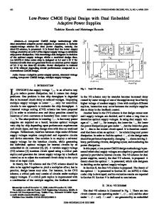
The proposed comparator in this paper is shown in the figure1. The Ibias defines the current in M3 and M4 as well as current in M5.It is likely that these current will not be exactly equal. If I3 is greater than I1, then M1 is saturated and M3 active. In this differential amplifier the design parameters are the W/L values of M1 through M5 and the current in M5.
increasing drain current of transistor M5 and decreasing compensation capacitor Cc. But when we increase the current in transistor M5 the DC gain start decreasing and power consumption will also increase. So we have to choose the appropriate vale of drain current of transistor M5. Gain of first stage
Av1
(1)
Gain of second stage
g m6 g ds 6 g ds 7 Total Gain ( AV ) AV 1 * AV 2 Av1
(2) (3)
g m1 Gain Bandwidth (GB) = C c Where g m1 , g ds 2 , g ds 4 , g m 6 , g ds 6
(4)
and
g ds 7
denote the transconductance of the MOS transistors M1, M2, M4, M6 and M7 respectively. Gain and Bandwidth of the system is important for high resolution and high speed operation. From the above equations Gain Bandwidth(GB) can be increase by increasing aspect ratio of transistor M1, M2 and its also depends on compensation capacitor(Cc).
3. DESIGN AND OPTIMIZATION OF CIRCUITS 3.1 Improve GB of Differential Comparator The gain bandwidth (GB) product should be high [3]. In the high speed comparator, the differential amplifier should have a wide bandwidth [7]. Meanwhile, it should have a high gain to amplify the input signals. GB can be increase by
g m1 g ds 2 g ds 4
————————————————
Chandan Singh is with National Institute of Technology, Jalandhar. A.Raman is with National Institute of Technology, Jalandhar.
© 2011 JCSE www.journalcse.co.uk
JOURNAL OF COMPUTER SCIENCE AND ENGINEERING, VOLUME 10, ISSUE 1, NOVEMBER 2011 14
preferable. This can be increase by increasing drain current of M7 transistor and aspect ratio of M6 transistor. It’s also depending on compensation capacitor Cc. By decreasing value of Cc can increase RHP Zero. The value of compensation capacitor is taken .1pF for adequate phase margin.
4.
In the circumstance of cadence composer, based on UMC 0.18um CMOS process model. The graphs (a), (b), (c) and (d) given below are of gain, propagation delay and power consumption and the observed value are 38dB, 22.23ps, 50µV and 474.54μW respectively. However, the mean value of the absolute value of the offset is approximately 17µV. The stability of the system can be done by selecting appropriate value of load capacitor for good phase margin
Figure-1 Two Stage Comparator using Nulling Resistor Compensation
TABLE I. COMPARISON OF SEVERAL COMPARATORS
3.2 Increasing Slew Rate
.
To get the faster response of the comparator it must have higher Slew Rate. Slew rate of given differential comparator is depends on aspect ratio of M5 transistor and compensation capacitor Cc. It can be increase by increasing the aspect ratio of M5 and decreasing the value of compensation capacitor Cc. Slew Rate (SR) = I/Cc (5) 3.3. Increasing RHP Zero The undesired RHP zero may not be negligible in paper [2]. It becomes necessary to employ the nulling resistor compensation. The RHP zero can be moved to the left half-plane by placing a resistor in series with the compensation capacitor. In fig-1, a compensation scheme using transistor M8 as a resistor has propose. This transistor is controlled by a control voltage Vb. The resulting poles and zeros are
p1
g m2 Av C c
p2
g m6 CL
Z1
RZ C c
g m1 Av C c
(6)
(7)
1 Cc g m6
Author
Resolution
Frequency
Power
Al-Rawi [9]
400µV
40MHz
1mW
Kotan i [10]
4mV
Not reported
4.3μW/(MS/s) (172μW @40 MHz)
Carlos J Solis [1]
1.8mV
40MHz
750µW
Proposed Design
50µV
45MHz
474.54µW
5.
1 C L CC g m6 Cc
CONCLUSION
The paper introduces a novel high resolution comparator using differential amplifier. The speed and the dynamic characteristics are also good. It is designed and simulated in a UMC 0.18um technology. The simulation results show its gain is 38dB, which is important for high resolution and propagation delay is 22.23ns it is suitable for high speed ADC. REFERENCES
(8)
[1]
where Rz is
RZ
SIMULATED RESULTS
[2]
(9)
The larger phase margin results in less ―ringing ―of the output signal[12]. The phase margin 60° is
[3]
© 2011 JCSE www.journalcse.co.uk
Carlos J Solis, Gladys O. Ducoudray, ―High Resolution Low Power 0.6μm CMOS 40MHz Dynamic Latch Comparator‖, IEEE Transactions on, vol. 978, no.1, pp. 4244-7773, Sept. 2010. Vladislav Y. Potanin, Ph.D. Elena E. Potanina, ―Analytical Optimization of a Multistage Amplifiers‖, IEEE Transactions on, vol. 9, no.1, pp. 4244-0173, Sept. 2006. M. Momeni, M. Glesner, ―A Class of Single-Stage and Multi-Stage LowpassDelta-Sigma Modulators in 1.2-V
JOURNAL OF COMPUTER SCIENCE AND ENGINEERING, VOLUME 10, ISSUE 1, NOVEMBER 2011 15
[4]
[5]
[6] [7]
0.13-μm CMOS‖, IEEE Transactions on, vol. 978, no.1, pp. 4244-5750, Oct. 2009. Yavuz De˘gerli, Nicolas Fourches, Michel Rouger, and Pierre Lutz, ―Low-Power Autozeroed High-Speed Comparator for the Readout Chain of a CMOS Monolithic Active Pixel Sensor Based Vertex Detector‖, IEEE Transactions on nuclear science , vol. 50, no.5, pp. 0018-9499, Oct. 2003. Lane Brooks, Hae-Seung Lee, ―A 12b, 50 MS/s, Fully Differential Zero-Crossing Based Pipelined ADC‖, IEEE Journal of Solid-State Circuits, VOL. 44, NO. 12, pp 0018-9200 Dec. 2009 Razavi B, Design of Analog CMOS Integrated Circuits, Mcgraw-Hill, 2001, pp 463-468 V.V. Ivanov, I. Filanovsky, "Operational amplifier speed and accuracy improvement: analog circuit design with structural methodology," Boston, Kluwer Academic
Publishers, 2004. Matthews, T.W.; , "On the effective sampling time of regenerative comparators, " Circuits and Systems, 2008. MWSCAS 2008. 51st Midwest Symposium on , vol., no., pp.638-641, 10-13 Aug. 2008. [9] Al-Rawi, G.A.; , "A new offset measurement and cancellation technique for dynamic latches," Circuits and Systems, 2002. ISCAS 2002. IEEE International Symposium on , vol.5, no., pp. V-149- V-152 vol.5, 2002 [10] Kotani, K.; Shibata, T.; Ohmi, T.; , "CMOS chargetransfer preamplifier for offset-fluctuation cancellation in low-power A/D converters," Solid-State Circuits, IEEE Journal of , vol.33, no.5,pp.762-769, May 1998. [11] Razavi, B.; Wooley, B.A.; , "Design techniques for highspeed, high resolution comparators," Solid-State Circuits, IEEE Journal of , vol.27, no.12, pp.1916-1926, Dec 1992. [12] Philip E. Allen; Douglas R.Holberg ― CMOS analog circuit design‖, International Second Edtion, Oxford University Publishers, 2010.
(a) Gain of comparator
[8]
(b) Propagation delay of comparator
(c)Transient analysis for offset calculation
Chandan Singh was born on May 25, 1986 at Gorakhpur, India. He did his B.Tech, (ECE), from BBDNITM Lucknow in 2009, M.Tech (VLSI Design) from NIT -Jalandhar under the guidance of Ashish Raman. He has interests in analog circuit designing, and has published papers in these areas Ashish Raman was born on May 15, 1983 at Moradabad, India. He did his BE ,(ECE), from MIT–Moradabad in 2003, M.Tech (Microelectronics and VLSI Design) from SGSITS -Indore in 2005. He has interests in semiconductors, microelectronics /VLSI, RF, Embedded System, DSP; and has published papers in these areas. He joined Electronics and Communication Engineering (ECE) Department of NIT-Jalandhar (India) in 2007. He has been working as Assistant Professor the ECE Department. He has been associated with IACSIT since 2010
© 2011 JCSE www.journalcse.co.uk
(d) Power consumption of comparator Figure 1 simulated results