INTERNATIONAL JOURNAL OF ELECTRICAL, ELECTRONICS AND COMPUTER SYSTEMS (IJEECS), Volume 1, Issue 2, April 2011. ISSN: 2221-7258(Print) ISSN: 2221-7266 (Online) www.ijeecs.org
4-BIT & 8-BIT FULL ADDER BY USING MODIFIED 8 TRANSISTORS N. M. Chore Bapurao Deshmukh College Of Engineering, Sevagram, Wardha, Maharashtra ,India
[email protected]
Abstract In this paper, a Modified low-voltage low power 8T one bit full adder circuit is proposed. The new design is by combining XOR gates. The current work proposes the design of the improved full adder using 8T which acquires less area and it most suitable for the cascading application such as Ripple Carry Adder. With the lowest number of transistor count. Based on the simulation results performed by Microwind Version 3.1, the new low voltage design consumes minimal power in 90 nm processes as supply voltage 1.2V and 180 nm processes as supply voltage 2V. This paper shows that carry signal voltage increased and Id(max) decreased by 48% & 22% for 180nm and 40% & 30% for 90nm technology. By using this one bit adder we design 4-bit and 8-bit adder modules. This module is compared with the 4-bit and 8bit CMOS full adder. The result shows that our modified full adder is better than the CMOS full adder in performance.
Index Terms – Full Adder, XOR Gate, Carry, Supply Voltage, Transistor Count.
1 Introduction The Explosive growth in laptop, portable system, and cellular networks has intensified the research efforts in low power microelectronics. Today we find number of portable applications requiring low power and high throughput circuits. Addition is one of the fundamental arithmetic operations. It is used extensively in many VLSI systems such as applicationspecific DSP architectures and microprocessors. In addition to its main task, which is adding two binary numbers, it is the nucleus of many other useful operations such as subtraction, multiplication, division, address calculation, etc. In most of these systems the adder is part of the critical path that determines the overall performance of the system. That is why enhancing the performance of the 1-bit full-adder cell (the building block of the binary adder) is a significant goal. Recently, building low-power VLSI systems has emerged as highly in demand because of the fast growing technologies in mobile communication and computation. The battery technology doesn’t advance at the same rate as the microelectronics technology. There is a limited amount of power available for the mobile systems. So designers are faced with more constraints: high speed, high throughput, small silicon
R. N. Mandavgane Bapurao Deshmukh College Of Engineering, Sevagram, Wardha, Maharashtra ,India
[email protected] area, and at the same time, low-power consumption [1]. So building low-power, high-performance adder cells is of great interest.
1.1 Power Consideration Designing systems aiming for low power is not a straightforward task, as it is involved in all the IC design stages beginning with the system behavioral description and ending with the fabrication and packaging processes. In some of these stages there are guidelines that are clear and there are steps to follow that reduce power consumption, such as decreasing the power-supply voltage. While in other stages there are no clear steps to follow, so statistical or probabilistic heuristic methods are used to estimate the power consumption of a given design [2], [3]. There are three major components of power dissipation in complementary metal–oxide– semiconductor (CMOS) circuits. 1) Switching Power: Power consumed by the circuit node capacitances during transistor switching. 2) Short Circuit Power: Power consumed because of the current flowing from power supply to ground during transistor switching. 3) Static Power: Due to leakage and static currents. The first two components are referred to as dynamic power. Dynamic power constitutes the majority of the power dissipated in CMOS VLSI circuits. It is the power dissipated during charging or discharging the load capacitances of a given circuit. It depends on the input pattern that will either cause the transistors to switch (consume dynamic power) or not to switch (no dynamic power consumed) at every clock cycle. It is given by the following in [4]:
Pdynamic =
(Ci Vi ( K . )(V load .
swing
. i ). fclk .Vdd
i
i
i
dd
2Vt )3 . fclk
i
And
Ki 12
Where,
Ciload load capacitance at node ; Viswing voltage swing;
INTERNATIONAL JOURNAL OF ELECTRICAL, ELECTRONICS AND COMPUTER SYSTEMS (IJEECS), Volume 1, Issue 2, April 2011. ISSN: 2221-7258(Print) ISSN: 2221-7266 (Online) www.ijeecs.org
i fclk Vdd Vt
switching activity factor; system clock frequency;
power supply voltage; transistor threshold voltage; gain factor of the transistor; rise or fall time of the signal. The summation is over all the nodes of the circuit. Reducing any of these components will end up with lower-power consumption, although, it is of equal importance to increase the system-clock frequency for faster operation. Estimating the power of a large circuit is a complex task. Heuristic algorithms, statistical, and probabilistic methods are used to generate randominput patterns to test the switching activity of the circuit. These methods become less accurate when the size of the circuit increases. It is better to decompose the large circuit into smaller modules and then use these methods to estimate the power consumption of each module. When the decomposed modules are small enough, exact methods can be used to optimize their performance. CAD tools and simulators could be used to build the circuit layout, simulate it, and estimate its power dissipation. Following this strategy, the best design of a given module is found and then by connecting the modules together the bigger circuit is formed, which will be optimized for low-power dissipation. The rest of the paper is organized as follows. In section II, we briefly describe the previous work reported in the literature. In section III, we propose the new improved 8T adder cell. Section IV, we present the simulation results and we draw the conclusion in section V.
2 Previous Work The survey of the Contemporary literature reveals very wide spectrum availability of adder designs over the decades. Several designs of low power adder cells can be found in the literature [5], [6], [7]. The transmission function full adder [8], which uses 16 transistors, for the realization of the circuit. For this circuit there are two possible short circuits paths to ground. This design uses pull-up and pull down logic as well as complementary pass Logic to drive the load. The dual value logic (DVL) full adder [9] illustrated uses 23 transistors for the realization of the adder function. The DVL was developed to improve the characteristics of double pass transistor logic, which was designed to have the logic level high signal passed to the load through a P transistor and the logic level low Drained from the load through an Ntransistor. The Fourteen transistors full adder [10], as the name implies, uses 14 Transistors to realize the adder function. The 14T full adder cell, like the transmission function full adder cell, implements the complementary pass logic to drive the load. The SERF design requires only 10 transistors to realize the adder
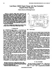
function. Even though it has threshold loss problem, it is suited for low power design so far. This design of full adder is based on three transistor XOR gates [11]. The design of a three transistor XOR gate is shown in figure.1 The design is based on a modified version of a CMOS inverter and a pass transistor when the input B is at logic high. The inverter, therefore the output Y is the complement of input A, when the input B is at logic low, the CMOS inverter output is at high impedance. However, the pass transistor M3 enabled and the output Y get the same logic value as input A. The Boolean equations for the design of the eight transistor full adder are as follows.
SUM A B CIN
COUT ( A ( AB )) (CIN ( A B ))
Figure.1 3T XOR GATE
The 8T transistor full adder design as shown in figure.2. This design required lowest number of transistor count. The 8T design has one logical problem in the design, the output of carry is degraded for combination of 101 sequence. For this sequence it has a feedback path from carry output to input terminal B that’s why it decrease the performance of the circuit.
Figure. 2 8T FULL ADDER
3 New Modified 8T Full Adder This design of modified full adder is again based on three transistor XOR gate as shown in figure.3. The new design avoids the problem of degraded carry out for combination of 101 sequence. This circuit shows the approximately 40% improvement in carry voltage as compare to previous 8T full adder design. For generation carry it uses multiplexer circuit. The maximum Id(max) is also decreased 30% for 180 nm and 22% for 90 nm.
INTERNATIONAL JOURNAL OF ELECTRICAL, ELECTRONICS AND COMPUTER SYSTEMS (IJEECS), Volume 1, Issue 2, April 2011. ISSN: 2221-7258(Print) ISSN: 2221-7266 (Online) www.ijeecs.org
8T carry Vs Modified 8T carry at 90nm 1.4 1.2 1 0.8
8T carry Proposed 8T carry
0.6
Fig. 3 MODIFIED 8T FULL ADDER
0.4 0.2
4 Simulation and Comparison
0 0
1
10
11
100
101
110
111
se que nc e
We have performed simulation using Microwind Version 3.1 in 90nm and 180nm technologies, with the supply voltage 1.2V for 90nm and 2V for 180nm technologies. To establish an impartial testing environment each circuit have been tested on the same input patterns. Comparative analysis on the different adders stated above have been done using 90nm and 180nm technologies. In our modified adder circuit we have reduced the aspect ratio of PMOS and NMOS transistor of Cout Module and as a result it shows the better performance. The result of the comparative study shows that the performance of 8T full adder is the best than the previous 8T full adder. The modified 8T full adder occupies the minimum silicon area on chip as compared to previous 8T full adder. The results of the simulation reveal that our modified 1-bit full adder cell is proven to be the best than the previous 8T full adder. Hence it has proven it superiority. 8T carry Vs Modified 8T carry at 180nm
Figure.5 8T carry Vs Modified 8T carry at 90nm
The above graphs depicts that the performance of modified 8T full adder is better than 8T full adder. This graph shows that carry signal voltage increased by 48% for 180nm and 40% for 90nm technology. Now we consider the area required for this adder is less than the all other full adder because it required less number of transistors from figure.6 [11].
Transistorcomparison 35 30
DVL
25
28TRANSISTOR
20
TRF
15
14T
10
SERF 8TNEW
5 2.5
0 1
2
Figure.6 TRANSISTOR COMPARISON 1.5 8T carry Proposed 8T carry 1
0.5
0 0
1
10
11
100
101
110
111
S e que nc e
Figure.4 8T carry Vs Modified 8T carry at 180nm
TABLE I Id(max) for 180nm & 90 nm Technology
INTERNATIONAL JOURNAL OF ELECTRICAL, ELECTRONICS AND COMPUTER SYSTEMS (IJEECS), Volume 1, Issue 2, April 2011. ISSN: 2221-7258(Print) ISSN: 2221-7266 (Online) www.ijeecs.org
Design
90nm Technology Id(max)
180nm Technology Id(max)
0.350mA
0.284mA
0.251mA
0.223mA
8T Adder
Modified 8T Adder
design an efficient and high performance multiplier unit. The modified 8T adder has been designed and studied using 180nm and 90nm technologies which establish the technologies independence of the circuit. By using this one bit adder we design 4-bit and 8-bit adder modules. This module is compared with the 4-bit and 8-bit CMOS full adder. The result shows that our modified full adder is better than the CMOS full adder in performance.
6 Reference The above table describe that the performance of modified 8T full adder is better than 8T full adder. This table shows that Id(max) decreased by 22% for 180nm and 30% for 90nm technology.
TABLE II Id(max) for 4-bit and 8 bit full adder in180nm Technology Adder design 4-bit CMOS 4-bit New 8-bit CMOS 8-bit new
Idd (Max) 4.044m A 0.641m A 4.064m A 0.641m A
P (Max)
Idd avg
8.088mW
0.407mA
1.282mW
0.215mA
8.128mW
0.397mA
1.282mW
0.215mA
P Avg 0.814m W 0.430m W 0.794m W 0.430m W
The table given above describe that the performance of 4-bit modified full adder is better than 4 bit CMOS full adder. Also, The below table describe that the performance of 8-bit New full adder is better than 8 bit CMOS full adder. This table shows that Idd (max) and Idd (avg) decreased by 84% and 47% for 180nm.
5 Conclusion The current work proposes the design of the improved full adder using 8T which acquires less area and it most suitable for the cascading application such as Ripple Carry Adder. With the lowest number of transistor count. It also reduces the threshold loss problem. With the help of this adder cell, we can
[1] N. Weste and K. Eshraghian, Principles of CMOS VLSI Design, ASystem Perspective. Reading, MA: AddisonWesley, 1993. [2] G. M. Blair, “Designing low-power CMOS,” Inst. Elect. Eng. Electron. Commun. Eng. J., vol. 6, pp. 229–236, Oct. 1994. [3] S. Devadas and S. Malik, “A survey of optimization techniques targeting low-power VLSI circuits,” in Proc. 32nd ACM/IEEE Design Automation Conf., San Francisco, CA, June 1995, pp. 242–247. [4] H. J. M. Veendrick, “Short-Circuit dissipation of static CMOS circuitry and its impact on the design of buffer circuits,” IEEE J. Solid-State Circuits, vol. SSC-19, pp. 468– 73, Aug. 1984. [5] R. Shalem, E. John, and L. K. John, “A novel low power energy recovery full adder cell,” in Proc. IEEE Great Lakes VLSI Symp., Feb. 1999, pp. 380–383. [6] R. Zimmermann and W. Fichtner, “Low-power logic styles: CMOS versus pass-transistor logic,” IEEE J. SolidState Circuits, vol. 32, pp.1079–1090, July 1997. [7] Nan Zhuang and Haomin Wu, “A new design of the CMOS full adder”IEEE Journal of Solid State Circuits, Vol. 27, No.5, pp. 840-844, May 1992. [8] V. G. Oklobdzija, M Soderstrand and B.Duchene “Development and Synthesis Method for Pass-Transistor Logic Family for High-Speed and Low Power CMOS” Proceedings of the 1995 IEEE 38th Midwest Symposium on Circuits and Systems, Rio de Janeiro, 1995. [9] Ahmed M. Shams and Magdy A. Bayoumi, “A New Full Adder Cell for low-power Applications”, Proceedings of the IEEE Great Lakes Symposium on VLSI, 1998, pp. 45-49. [10] Shubhajit Roy Choudhary, Aritra Banerjee, Anirudha Roy, Hiranmay saha, “ A high speed 8 transistor full adder design using Novel 3 transistor XOR gates” in International journal of electronics, Circuits and systems 2;4 @ www.waset.org Fall 2008. [11] T. Vigneswaran, B. Mukundhan, and P. Subbarami Reddy, “A Novel Low Power, High Speed 14 Transistor CMOS Full Adder Cell with 50% Improvement in Threshold Loss Problem” in World Academy of Science, Engineering and Technology 13 2006.